XINETRON, INC.
XI222
|
NIC Type |
ARCnet |
|
Transfer Rate |
2.5Mbps |
|
Data Bus |
16-bit ISA |
|
Topology |
Star Linear bus |
|
Wiring Type |
Shielded/Unshielded Twisted Pair |
|
Boot ROM |
Available |
|
NODE ADDRESS |
||||||||
|
Node |
SW2/1 |
SW2/2 |
SW2/3 |
SW2/4 |
SW2/5 |
SW2/6 |
SW2/7 |
SW2/8 |
|
0 |
- |
- |
- |
- |
- |
- |
- |
- |
|
1 |
On |
On |
On |
On |
On |
On |
On |
Off |
|
2 |
On |
On |
On |
On |
On |
On |
Off |
On |
|
3 |
On |
On |
On |
On |
On |
On |
Off |
Off |
|
4 |
On |
On |
On |
On |
On |
Off |
On |
On |
|
251 |
Off |
Off |
Off |
Off |
Off |
On |
Off |
Off |
|
252 |
Off |
Off |
Off |
Off |
Off |
Off |
On |
On |
|
253 |
Off |
Off |
Off |
Off |
Off |
Off |
On |
Off |
|
254 |
Off |
Off |
Off |
Off |
Off |
Off |
Off |
On |
|
255 |
Off |
Off |
Off |
Off |
Off |
Off |
Off |
Off |
|
Note: Node address 0 is used for messaging between nodes and must not be used. A total of 255 node address settings are available. The switches are a binary representation of the decimal node addresses. Switch 8 is the Least Significant Bit and switch 1 is the Most Significant Bit. The switches have the following decimal values: switch 1=128, 2=64, 3=32, 4=16, 5=8, 6=4, 7=2, 8=1. Turn off the switches and add the values of the off switches to obtain the correct node address. (On=0, Off=1) |
||||||||
|
RESPONSE AND RECONFIGURATION TIMEOUTS |
|||||
|
Response Time |
Ide Time |
Reconfiguration Time |
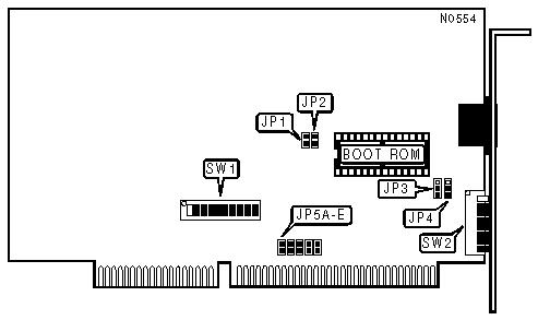
JP1 |
JP2 |
|
|
» |
78µs |
86µs |
840ms |
Open |
Open |
|
|
285µs |
316µs |
1680ms |
Open |
Closed |
|
|
563µs |
624µs |
1680ms |
Closed |
Open |
|
|
1130µs |
1237µs |
1680ms |
Closed |
Closed |
|
Note: All NICs on the network segment must have this option set the same. |
|||||
|
TWISTED PAIR CONFIGURATION |
||
|
Wire Pair |
JP3 |
JP4 |
|
Network uses first pair (two inside wires on connector) |
Pins 2 & 3 closed |
Pins 2 & 3 closed |
|
Network uses second pair (two outside wires on connector) |
Pins 1 & 2 closed |
Pins 1 & 2 closed |
|
Note: This table assumes that the cable used is RJ-11 in a 4-wire arrangement. |
||
|
INTERRUPT REQUEST |
||||||
|
IRQ |
JP5A |
JP5A |
JP5A |
JP5A |
JP5A |
|
|
» |
2 |
Closed |
Open |
Open |
Open |
Open |
|
|
3 |
Open |
Closed |
Open |
Open |
Open |
|
|
4 |
Open |
Open |
Closed |
Open |
Open |
|
|
5 |
Open |
Open |
Open |
Closed |
Open |
|
|
7 |
Open |
Open |
Open |
Open |
Closed |
|
I/O BASE ADDRESS |
|||||||
|
Address |
SW1/1 |
SW1/2 |
SW1/3 |
SW1/4 |
SW1/5 |
SW1/6 |
|
|
|
260-26Fh |
Off |
On |
On |
Off |
Off |
On |
|
|
290-29Fh |
Off |
On |
Off |
On |
On |
Off |
|
» |
2E0-2EFh |
Off |
On |
Off |
Off |
Off |
On |
|
|
2F0-2FFh |
Off |
On |
Off |
Off |
Off |
Off |
|
|
300-30Fh |
Off |
Off |
On |
On |
On |
On |
|
|
350-35Fh |
Off |
Off |
On |
Off |
On |
Off |
|
|
380-38Fh |
Off |
Off |
Off |
On |
On |
On |
|
|
3E0-3EFh |
Off |
Off |
Off |
Off |
Off |
On |
|
BASE MEMORY ADDRESS AND BOOT ROM ADDRESS |
||||||
|
Base Address |
Boot ROM Address |
SW1/7 |
SW1/8 |
SW1/9 |
SW1/10 |
|
|
|
C0000-C07FFh |
C2000-C3FFFh |
Off |
Off |
On |
On |
|
» |
D0000-D07FFh |
D2000-D3FFFh |
Off |
Off |
On |
Off |
|
|
E0000-E07FFh |
E2000-E3FFFh |
Off |
Off |
Off |
On |
|
DIAGNOSTIC LED |
|||
|
LED |
Color |
Status |
Condition |
|
LED1 |
Yellow |
Blinking |
Card is not connected to network |
|
LED1 |
Yellow |
On |
Normal operation |
|
LED1 |
Yellow |
Flashing |
Data is being transmitted/received |
|
Note: Location of LED1 is unknown. |
|||