VTECH INDUSTRIES, INC.
LASER 386SX/2, 386SX/3
|
Device Type |
Mainboard |
|
Processor |
80386SX |
|
Processor Speed |
16/20/25MHz |
|
Chip Set |
Unidentified |
|
Video Chip Set |
None |
|
Maximum Onboard Memory |
4MB |
|
Maximum Video Memory |
None |
|
Cache |
None |
|
BIOS |
Unidentified |
|
Dimensions |
305mm x 244mm |
|
I/O Options |
Floppy drive interface, game port, IDE interface, serial ports (2), parallel port |
|
NPU Options |
80387SX |
|
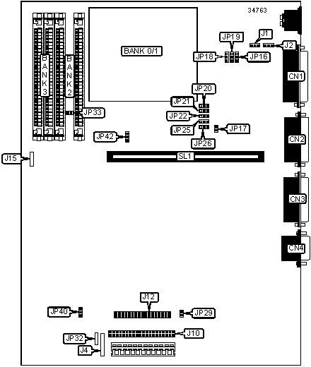
CONNECTIONS | |||
|
Purpose |
Location |
Purpose |
Location |
|
Parallel port |
CN1 |
IDE interface |
J10 |
|
Game port |
CN2 |
Floppy drive interface |
J12 |
|
Serial port |
CN3 |
Speaker |
J15 |
|
Serial port |
CN4 |
IDE interface LED |
JP32 |
|
Front panel connector |
J4 |
Riser slot |
SL1 |
|
USER CONFIGURABLE SETTINGS | |||
|
Function |
Label |
Position | |
|
» |
Factory configured - do not alter |
J1 |
Unidentified |
|
» |
Factory configured - do not alter |
J2 |
Unidentified |
|
» |
Factory configured - do not alter |
JP17 |
Unidentified |
|
Floppy drive interface enabled |
JP28 |
Open | |
|
Floppy drive interface disabled |
JP28 |
Closed | |
|
IDE interface enabled |
JP29 |
Closed | |
|
IDE interface disabled |
JP29 |
Open | |
|
Parity enabled |
JP33 |
Closed | |
|
Parity disabled |
JP33 |
Open | |
|
NPU not installed |
JP40 |
Pins 1 & 2 closed | |
|
NPU installed |
JP40 |
Pins 2 & 3 closed | |
|
Interleave mode enabled |
JP42 |
Pins 1 & 2 closed | |
|
Interleave mode disabled |
JP42 |
Pins 2 & 3 closed | |
|
Note: The location of JP28 is unidentified. | |||
|
MEMORY CONFIGURATION | ||||
|
Size |
Bank 0 |
Bank 1 |
Bank 2 |
Bank 3 |
|
1MB |
44256 |
44256 |
None |
None |
|
1.5MB |
44256 |
44256 |
(2) 256K x 9 |
None |
|
2MB (A) |
44256 |
44256 |
(2) 256K x 9 |
(2) 256K x 9 |
|
2MB (B) |
None |
None |
(2) 1M x 9 |
None |
|
4MB |
None |
None |
(2) 1M x 9 |
(2) 1M x 9 |
|
Note: The number of 44256 chips is unidentified. Parity chips are 4464. The location and amount of chips used is unidentified. | ||||
|
MEMORY SWITCH CONFIGURATION | |||||
|
Size |
SW1/1 |
SW1/2 |
SW1/3 |
SW1/4 |
SW1/5 |
|
1MB |
On |
On |
On |
Off |
On |
|
1.5MB |
On |
On |
On |
Off |
On |
|
2MB (A) |
On |
On |
On |
Off |
On |
|
2MB (B) |
On |
Off |
Off |
Off |
On |
|
4MB |
On |
Off |
Off |
Off |
On |
|
Note: The location of the switch is unidentified. | |||||
|
MEMORY SWITCH CONFIGURATION (CON’T) | |||||
|
Size |
SW1/6 |
SW1/7 |
SW1/8 |
SW1/9 |
SW1/10 |
|
1MB |
On |
Off |
On |
On |
Off |
|
1.5MB |
On |
Off |
On |
Off |
On |
|
2MB (A) |
On |
Off |
On |
Off |
Off |
|
2MB (B) |
On |
Off |
On |
On |
On |
|
4MB |
On |
Off |
On |
On |
Off |
|
Note: The location of the switch is unidentified. | |||||
|
SERIAL PORT INTERRUPT SELECTION | ||||
|
IRQ |
JP18 |
JP19 |
JP20 |
JP22 |
|
25-pin port as COM1, IRQ4. 9-pin port COM2, IRQ3 |
1 & 2 |
2 & 3 |
2 & 3 |
1 & 2 |
|
25-pin port as COM2, IRQ3. 9-pin port COM1, IRQ4 |
2 & 3 |
1 & 2 |
1 & 2 |
2 & 3 |
|
Note: Pins designated should be in the closed position. JP25 & JP26 are used to set 3E8 and 2E8. The configuration is unidentified. | ||||
|
PARALLEL PORT INTERRUPT SELECTION | ||
|
IRQ |
JP16 |
JP21 |
|
IRQ7 |
Pins 2 & 3 closed |
Pins 1 & 2 closed |
|
IRQ5 |
Pins 1 & 2 closed |
Pins 2 & 3 closed |
|
Disabled |
Open |
Open |