WUGO (DELL)
PREMIER-286
|
Processor |
80286 |
|
Processor Speed |
8/12MHZ |
|
Chip Set |
VLSI |
|
Max. onboard DRAM |
4MB |
|
SRAM Cache |
None |
|
BIOS |
Award/Phoenix |
|
Dimensions |
330mm x 218mm |
|
I/O Options |
None |
|
NPU Options |
None |
|
CONNECTIONS | |||
|
Purpose |
Location |
Purpose |
Location |
|
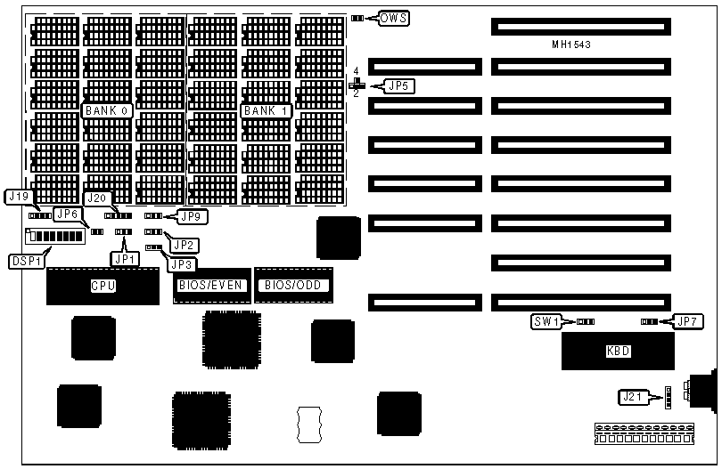
Speaker |
J19 |
External battery |
J21 |
|
Power LED & keylock |
J20 | ||
|
USER CONFIGURABLE SETTINGS | |||
|
Function |
Jumper/Switch |
Position | |
| » |
Clock speed select low |
DSP1/switch 1 |
On |
|
Clock speed select high |
DSP1/switch 1 |
Off | |
| » |
Factory configured - do not alter |
DSP1/switch 2 |
On |
| » |
I/O bus speed select 4 wait states |
DSP1/switch 3 |
On |
|
I/O bus speed select 6 wait states |
DSP1/switch 3 |
Off | |
| » |
EMS port select address OE8h |
DSP1/switch 4 |
On |
|
EMS port select address O98h |
DSP1/switch 4 |
Off | |
| » |
Turbo switch select external |
JP1 |
pins 1 & 2 closed |
|
Turbo switch select internal via DSP1/switch 1 |
JP1 |
pins 2 & 3 closed | |
| » |
Factory configured - do not alter |
JP2 |
pins 2 & 3 closed |
| » |
I/O wait state select synchronous with system clock |
JP3 |
pins 1 & 2 closed |
|
I/O wait state select internal via DSP1/switch 3 |
JP3 |
pins 2 & 3 closed | |
| » |
Factory configured - do not alter |
JP4 |
Open |
| » |
Request interrupt timing select standard |
JP5 |
pins 1 & 2 closed |
|
Request interrupt timing select fast (HDD/FDD) |
JP5 |
pins 2 & 3 closed | |
|
Request interrupt timing select slow (TRQ delay) |
JP5 |
pins 2 & 4 closed | |
| » |
Factory configured - do not alter |
JP6 |
Open |
| » |
Keyboard BIOS type select Award |
JP7 |
pins 2 & 3 closed |
| » |
Keyboard BIOS type select Phoenix |
JP7 |
pins 1 & 2 closed |
| » |
EMS switch select external |
JP8 |
Closed |
|
EMS switch select internal via DSP1/switch 4 |
JP8 |
Open | |
| » |
Power good signal detect from power supply |
JPF |
pins 2 & 3 closed |
|
Power good signal detect from board |
JPF |
pins 1 & 2 closed | |
| » |
Memory select 0 wait states |
OWS |
Closed |
|
Memory select 1 wait state |
OWS |
Open | |
| » |
Monitor type select color |
SW1 |
pins 2 & 3 closed |
|
Monitor type select monochrome |
SW1 |
pins 1 & 2 closed | |
|
Note:The locations of jumpers JP4, JP8, and JPF are unknown. | |||
|
DRAM SIZE CONFIGURATION | |||||||
|
Total DRAM |
Base |
EMS |
Bank 0 |
Bank 1 |
DSP1/6 |
DSP1/7 |
DSP1/8 |
|
512KB |
512KB |
NONE |
(18) 41256 |
NONE |
On |
On |
On |
|
640KB |
640KB |
NONE |
(18) 41256 |
(18) 4164 |
On |
On |
Off |
|
1MB |
640KB |
384KB |
(18) 41256 |
(18) 41256 |
On |
Off |
On |
|
1MB |
1024KB |
NONE |
(18) 41256 |
(18) 41256 |
On |
Off |
Off |
|
2MB |
640KB |
1408KB |
(18) 411000 |
NONE |
Off |
On |
On |
|
2MB |
2048KB |
NONE |
(18) 411000 |
NONE |
Off |
On |
Off |
|
4MB |
640KB |
3456KB |
(18) 411000 |
(18) 411000 |
Off |
Off |
On |
|
4MB |
4096KB |
NONE |
(18) 411000 |
(18) 411000 |
Off |
Off |
Off |
|
BIOS TYPE CONFIGURATION | ||
|
Type |
DSP1/switch 5 |
JP9 |
|
27128 |
On |
pins 1 & 2 closed |
|
27256 |
Off |
pins 2 & 3 closed |