UNIDENTIFIED
CACHE-386
|
Processor |
80386DX |
|
Processor Speed |
25MHz |
|
Chip Set |
ZYMOS Poach |
|
Max. Onboard DRAM |
16MB |
|
Cache |
32KB |
|
BIOS |
Unidentified |
|
Dimensions |
355mm x 304mm |
|
I/O Options |
None |
|
NPU Options |
80387/3167 |
|
CONNECTIONS | |||
|
Purpose |
Location |
Purpose |
Location |
|
Power LED & keylock |
J17 |
Speaker |
J20 |
|
External keyboard |
J18 |
Turbo LED |
Unidentified |
|
Reset switch |
J19 |
External battery |
Unidentified |
|
USER CONFIGURABLE SETTINGS | |||
|
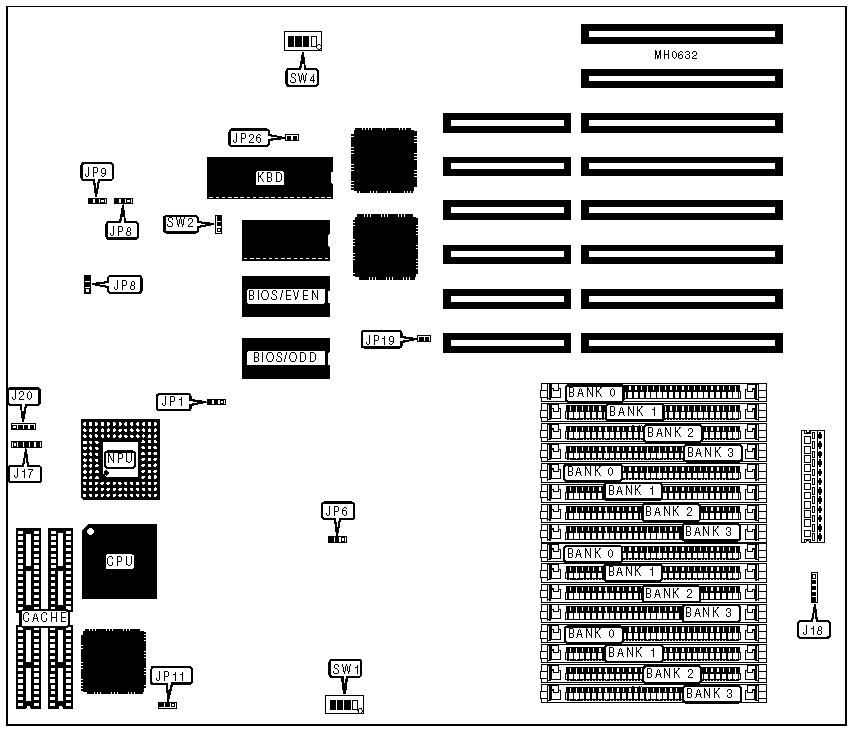
Function |
Jumper |
Position | |
| » |
NPU mode select asynchronous with CPU |
JP1 |
pins 2 & 3 closed |
|
NPU mode select synchronous with CPU |
JP1 |
pins 1 & 2 closed | |
| » |
Factory configured - do not alter |
JP2 |
N/A |
| » |
Factory configured - do not alter |
JP3 |
N/A |
| » |
Factory configured - do not alter |
JP4 |
N/A |
| » |
Factory configured - do not alter |
JP5 |
N/A |
| » |
Factory configured - do not alter |
JP10 |
N/A |
| » |
Pipeline mode enabled |
JP11 |
pins 1 & 2 closed |
|
Pipeline mode disabled |
JP11 |
pins 2 & 3 closed | |
| » |
Factory configured - do not alter |
JP22 |
N/A |
| » |
Factory configured - do not alter |
JP25 |
N/A |
| » |
CPU speed select fast (25MHz) |
JP26 |
Open |
|
CPU speed select slow (8MHz) |
JP26 |
pins 1 & 2 closed | |
| » |
Monitor type select color |
SW2 |
pins 1 & 2 closed |
|
Monitor type select monochrome |
SW2 |
pins 2 & 3 closed | |
|
DRAM CONFIGURATION | ||||
|
Size |
Bank 0 |
Bank 1 |
Bank 2 |
Bank 3 |
|
1MB |
(4) 256K x 9 |
NONE |
NONE |
NONE |
|
1MB(EMS) |
(4) 256K x 9 |
NONE |
NONE |
NONE |
|
2MB |
(4) 256K x 9 |
(4) 256K x 9 |
NONE |
NONE |
|
3MB |
(4) 256K x 9 |
(4) 256K x 9 |
(4) 256K x 9 |
NONE |
|
4MB |
(4) 256K x 9 |
(4) 256K x 9 |
(4) 256K x 9 |
(4) 256K x 9 |
|
4MB (EMS) |
(4) 1M x 9 |
NONE |
NONE |
NONE |
|
5MB |
(4) 1M x 9 |
(4) 256K x 9 |
NONE |
NONE |
|
6MB |
(4) 1M x 9 |
(4) 256K x 9 |
(4) 256K x 9 |
NONE |
|
7MB |
(4) 1M x 9 |
(4) 256K x 9 |
(4) 256K x 9 |
(4) 256K x 9 |
|
8MB |
(4) 1M x 9 |
(4) 1M x 9 |
NONE |
NONE |
|
9MB |
(4) 1M x 9 |
(4) 1M x 9 |
(4) 256K x 9 |
NONE |
|
10MB |
(4) 1M x 9 |
(4) 1M x 9 |
(4) 256K x 9 |
(4) 256K x 9 |
|
12MB |
(4) 1M x 9 |
(4) 1M x 9 |
(4) 1M x 9 |
NONE |
|
12MB (EMS) |
(4) 1M x 9 |
(4) 1M x 9 |
(4) 1M x 9 |
NONE |
|
13MB |
(4) 1M x 9 |
(4) 1M x 9 |
(4) 1M x 9 |
(4) 256K x 9 |
|
16MB |
(4) 1M x 9 |
(4) 1M x 9 |
(4) 1M x 9 |
(4) 1M x 9 |
|
16MB (EMS) |
(4) 1M x 9 |
(4) 1M x 9 |
(4) 1M x 9 |
(4) 1M x 9 |
|
DRAM SWITCH CONFIGURATION | ||||
|
Size |
SW4/1 |
SW4/2 |
SW4/3 |
SW4/4 |
|
1MB |
On |
On |
On |
On |
|
1MB(EMS) |
Off |
On |
On |
On |
|
2MB |
On |
Off |
On |
On |
|
3MB |
Off |
Off |
On |
On |
|
4MB |
On |
On |
Off |
On |
|
4MB (EMS) |
On |
On |
Off |
On |
|
5MB |
Off |
On |
Off |
On |
|
6MB |
On |
Off |
Off |
On |
|
7MB |
Off |
Off |
Off |
On |
|
8MB |
On |
On |
On |
Off |
|
9MB |
Off |
On |
On |
Off |
|
10MB |
On |
Off |
On |
Off |
|
12MB |
Off |
Off |
On |
Off |
|
12MB (EMS) |
On |
On |
Off |
Off |
|
13MB |
Off |
On |
Off |
Off |
|
16MB |
On |
Off |
Off |
Off |
|
16MB (EMS) |
Off |
Off |
Off |
Off |
|
DRAM TYPE CONFIGURATION | |||||
|
Bank |
DRAM type |
SW1/1 |
SW1/2 |
SW1/3 |
SW1/4 |
|
Bank 0 |
256K x 9 |
On |
N/A |
N/A |
N/A |
|
Bank 0 |
1M x 9 |
Off |
N/A |
N/A |
N/A |
|
Bank 1 |
256K x 9 |
N/A |
On |
N/A |
N/A |
|
Bank 1 |
1M x 9 |
N/A |
Off |
N/A |
N/A |
|
Bank 2 |
256K x 9 |
N/A |
N/A |
On |
N/A |
|
Bank 2 |
1M x 9 |
N/A |
N/A |
Off |
N/A |
|
Bank 3 |
256K x 9 |
N/A |
N/A |
N/A |
On |
|
Bank 3 |
1M x 9 |
N/A |
N/A |
N/A |
Off |
|
DRAM MODE CONFIGURATION | ||
|
Size |
JP7 |
JP9 |
|
Bypass |
pins 2 & 3 closed |
pins 2 & 3 closed |
|
Normal |
pins 1 & 2 closed |
pins 1 & 2 closed |
|
CACHE CONFIGURATION |
|
Note: The size of the cache chips are unidentified. Maximum cache size is 32KB. |
|
NPU CONFIGURATION | ||
|
Setting |
JP6 |
JP8 |
|
Disabled |
pins 1 & 2 closed |
pins 1 & 2 closed |
|
Enabled |
pins 2 & 3 closed |
pins 2 & 3 closed |