UNIDENTIFIED
SUPER 286
|
Processor |
80286 |
|
Processor Speed |
12MHz |
|
Chip Set |
Unidentified |
|
Max. Onboard DRAM |
4MB |
|
Cache |
None |
|
BIOS |
AMI/Award/ERSO/Phoenix |
|
Dimensions |
330mm x 218mm |
|
I/O Options |
None |
|
NPU Options |
80287 |
|
CONNECTIONS | |||
|
Purpose |
Location |
Purpose |
Location |
|
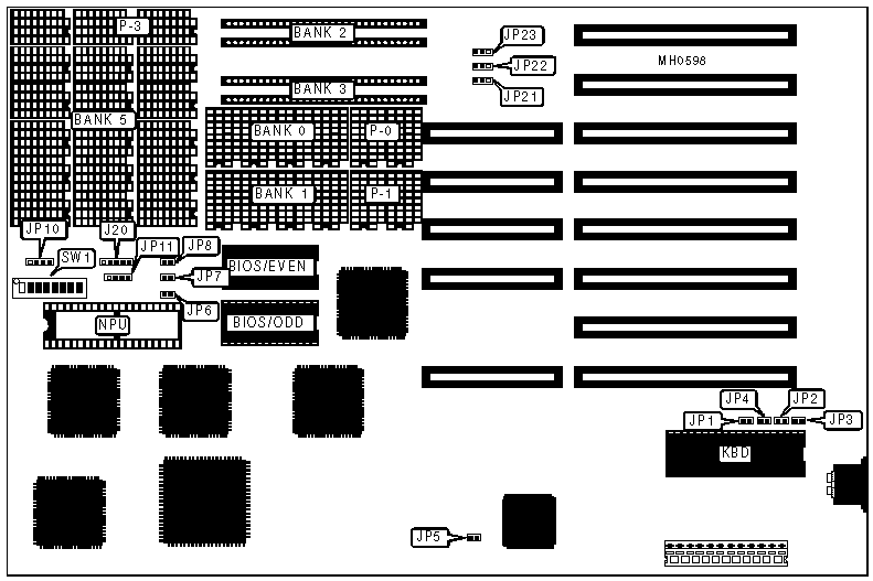
Power LED & keylock |
J20 |
Turbo LED |
JP8 |
|
Reset switch |
JP6 |
Speaker |
JP10 |
|
Turbo switch |
JP7 |
External battery |
JP11 |
|
USER CONFIGURABLE SETTINGS | |||
|
Function |
Jumper/Switch |
Position | |
| » |
BIOS type select Phoenix |
JP1 |
Closed |
|
BIOS type select Award |
JP3 |
Closed | |
| » |
DRAM wait states select 0 wait states |
JP5 |
Closed |
|
DRAM wait state select 1 wait state |
JP5 |
Open | |
| » |
CPU speed select switchable at keyboard (boot slow) [CTRL][ALT][-] slow speed (Award BIOS) [CTRL][ALT][+] fast speed (Award BIOS) [CTRL][ALT[\] toggle speeds (Phoenix BIOS) |
JP7 |
Open |
|
CPU speed select forced fast |
JP7 |
Closed | |
| » |
Monitor type select color |
SW1/2 |
On |
|
Monitor type select monochrome |
SW1/2 |
Off | |
| » |
EMS port address select 098-09FH |
SW1/4 |
Off |
|
EMS port address select 0E8-0EFH |
SW1/4 |
On | |
| » |
BIOS type select 27256 |
SW1/5 |
Off |
|
BIOS type select 27128 |
SW1/5 |
On | |
|
DRAM CONFIGURATION | |||||
|
Size |
Bank 0 |
Bank 1 |
Bank 2 |
Bank 3 |
Bank 5 |
|
512KB 1 |
NONE |
NONE |
NONE |
NONE |
(16) 41256 |
|
512KB 2 |
(4) 44256 |
NONE |
NONE |
NONE |
NONE |
|
512KB 3 |
NONE |
NONE |
(2) 256K x 9 |
NONE |
NONE |
|
640KB 1 |
(4) 44256 |
NONE |
NONE |
NONE |
(16) 4164 |
|
640KB 2 |
NONE |
NONE |
(2) 256K x 9 |
NONE |
(16) 4164 |
|
1MB 1 |
(4) 44256 |
(4) 44256 |
NONE |
NONE |
NONE |
|
1MB 2 |
NONE |
NONE |
(2) 256K x 9 |
(2) 256K x 9 |
NONE |
|
1MB 3 |
(4) 44256 |
NONE |
NONE |
NONE |
(16) 41256 |
|
1MB 4 |
NONE |
NONE |
(2) 256K x 9 |
NONE |
(16) 41256 |
|
1MB 5 |
NONE |
(4) 44256 |
NONE |
NONE |
(16) 41256 |
|
1MB 6 |
NONE |
NONE |
NONE |
(2) 256K x 9 |
(16) 41256 |
|
2MB 1 |
NONE |
NONE |
NONE |
NONE |
(16) 411000 |
|
2MB 2 |
NONE |
NONE |
(2) 1M x 9 |
NONE |
NONE |
|
4MB 1 |
NONE |
NONE |
(2) 1M x 9 |
(2) 1M x 9 |
NONE |
|
4MB 2 |
NONE |
NONE |
(2) 1M x 9 |
NONE |
(16) 411000 |
|
4MB 3 |
NONE |
NONE |
NONE |
(2) 1M x 9 |
(16) 411000 |
|
Note:Reference the next table for the proper parity configurations. | |||||
|
DRAM PARITY CONFIGURATION | |||
|
Size |
P-0 |
P-1 |
P-3 |
|
512KB 1 |
NONE |
NONE |
(2) 41256 |
|
512KB 2 |
(2) 41256 |
NONE |
NONE |
|
640KB 1 |
(2) 41256 |
NONE |
(2) 4164 |
|
640KB 2 |
NONE |
NONE |
(2) 4164 |
|
1MB 1 |
(2) 41256 |
(2) 41256 |
NONE |
|
1MB 3 |
(2) 41256 |
NONE |
(2) 41256 |
|
1MB 4 |
NONE |
NONE |
(2) 41256 |
|
1MB 5 |
(2) 41256 |
NONE |
(2) 41256 |
|
1MB 6 |
NONE |
NONE |
(2) 41256 |
|
2MB 1 |
NONE |
NONE |
(2) 411000 |
|
4MB 2 |
NONE |
NONE |
(2) 411000 |
|
4MB 3 |
NONE |
NONE |
(2) 411000 |
|
Note:Reference the previous table for the proper DRAM configurations. | |||
|
DRAM JUMPER/SWITCH CONFIGURATION | ||||||
|
Size |
SW1/6 |
SW1/7 |
SW1/8 |
JP21 |
JP22 |
JP23 |
|
512KB |
On |
On |
On |
1 & 2 |
1 & 2 |
1 & 2 |
|
640KB |
On |
On |
Off |
2 & 3 |
2 & 3 |
2 & 3 |
|
1MB |
On |
Off |
On |
2 & 3 |
2 & 3 |
2 & 3 |
|
1MB |
On |
Off |
On |
1 & 2 |
1 & 2 |
1 & 2 |
|
2MB |
Off |
On |
On |
1 & 2 |
1 & 2 |
1 & 2 |
|
4MB |
Off |
Off |
On |
2 & 3 |
2 & 3 |
2 & 3 |
|
4MB |
Off |
Off |
On |
1 & 2 |
1 & 2 |
1 & 2 |
|
Note:Pins designated should be in the closed position. | ||||||
|
EMS SWITCH CONFIGURATION | |||
|
Size(640KB base) |
SW1/6 |
SW1/7 |
SW1/8 |
|
+EMS (384KB) |
On |
Off |
Off |
|
+EMS (1408KB) |
Off |
On |
Off |
|
+EMS (3456KB) |
Off |
Off |
Off |