TANDY/RADIO SHACK
425SX/T, 433SX/T, 433DX/T, 450DX2/T, 466DX2/T
|
Processor |
80486SX/ODP486SX/80487SX/80486DX/ODP486SX/80486DX2 |
|
Processor Speed |
25/33/50(internal)/66(internal)MHz |
|
Chip Set |
Unidentified |
|
Video Chip Set |
Unidentified |
|
Maximum Onboard Memory |
40MB |
|
Maximum Video Memory |
1MB |
|
Cache |
64/128/256KB |
|
BIOS |
Phoenix |
|
Dimensions |
330mm x 218mm |
|
I/O Options |
Floppy drive interface, IDE interface, parallel port, PS/2 mouse port, serial ports (2), VGA feature connector, VGA port, riser slot |
|
NPU Options |
None |
|
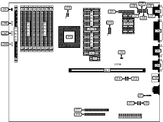
CONNECTIONS | |||
|
Purpose |
Location |
Purpose |
Location |
|
VGA port |
CN1 |
Reset switch |
CN8 |
|
Parallel port |
CN2 |
External battery |
J7 |
|
Serial port 1 |
CN3 |
IDE interface |
J17 |
|
Serial port 2 |
CN4 |
Floppy drive interface |
J18 |
|
PS/2 mouse port |
CN5 |
VGA feature connector |
J21 |
|
IDE interface LED |
CN6 |
Riser slot |
SL1 |
|
Power LED & keylock |
CN7 | ||
|
USER CONFIGURABLE SETTINGS | |||
|
Function |
Label |
Position | |
|
» |
Factory configured - do not alter |
J9 |
Pins 1 & 2 closed |
|
» |
Factory configured - do not alter |
J11 |
Open |
|
» |
Factory configured - do not alter |
J13 |
Pins 1 & 2 closed |
|
» |
Factory configured - do not alter |
J14 |
Pins 2 & 3 closed |
|
» |
CMOS memory normal operation |
J20 |
Closed |
|
CMOS memory clear |
J20 |
Open | |
|
» |
On board video enabled |
J28 |
Pins 2 & 3 closed |
|
On board video disabled |
J28 |
Pins 1 & 2 closed | |
|
» |
Factory configured - do not alter |
J29 |
Open |
|
» |
Floppy drive write protect disabled |
J30 |
Pins 2 & 3 closed |
|
Floppy drive write protect enabled |
J30 |
Pins 1 & 2 closed | |
|
» |
Factory configured - do not alter |
J31 |
Pins 2 & 3 closed |
|
» |
Zero wait state enabled |
J32 |
Closed |
|
Zero wait state disabled |
J32 |
Open | |
|
DRAM CONFIGURATION | |||
|
Size |
Bank 0 |
Bank 1 |
Bank 2 |
|
1MB |
(1) 256K x 36 |
None |
None |
|
2MB |
None |
(4) 256K x 9 |
(4) 256K x 9 |
|
2MB |
(1) 512K x 36 |
None |
None |
|
4MB |
None |
(4) 1M x 9 |
None |
|
4MB |
(1) 1M x 36 |
None |
None |
|
5MB |
None |
(4) 1M x 9 |
(4) 256K x 9 |
|
6MB |
(1) 512K x 36 |
(4) 1M x 9 |
None |
|
8MB |
(1) 1M x 36 |
(4) 1M x 9 |
None |
|
8MB |
(1) 2M x 36 |
None |
None |
|
8MB |
None |
(4) 1M x 9 |
(4) 1M x 9 |
|
10MB |
(1) 512K x 36 |
(4) 1M x 9 |
(4) 1M x 9 |
|
12MB |
(1) 1M x 36 |
(4) 1M x 9 |
(4) 1M x 9 |
|
12MB |
(1) 2M x 36 |
(4) 1M x 9 |
None |
|
16MB |
(1) 2M x 36 |
(4) 1M x 9 |
(4) 1M x 9 |
|
16MB |
None |
(4) 4M x 9 |
None |
|
DRAM CONFIGURATION (CON’T) | |||
|
Size |
Bank 0 |
Bank 1 |
Bank 2 |
|
17MB |
None |
(4) 4M x 9 |
(4) 256K x 9 |
|
18MB |
(1) 512K x 36 |
(4) 4M x 9 |
None |
|
20MB |
(1) 1M x 36 |
(4) 4M x 9 |
None |
|
20MB |
None |
(4) 4M x 9 |
(4) 1M x 9 |
|
22MB |
(1) 512K x 36 |
(4) 4M x 9 |
(4) 1M x 9 |
|
24MB |
(1) 1M x 36 |
(4) 4M x 9 |
(4) 1M x 9 |
|
24MB |
(1) 2M x 36 |
(4) 4M x 9 |
None |
|
28MB |
(1) 2M x 36 |
(4) 4M x 9 |
(4) 1M x 9 |
|
32MB |
None |
(4) 4M x 9 |
(4) 4M x 9 |
|
34MB |
(1) 512K x 36 |
(4) 4M x 9 |
(4) 4M x 9 |
|
36MB |
(1) 1M x 36 |
(4) 4M x 9 |
(4) 4M x 9 |
|
40MB |
(1) 2M x 36 |
(4) 4M x 9 |
(4) 4M x 9 |
|
CACHE CONFIGURATION | ||||
|
Size |
Bank 0 |
Bank 1 |
TAG |
U1 |
|
64KB |
(4) 8K x 8 |
(4) 8K x 8 |
(1) 8K x 8 |
(1) 64K x 1 |
|
128KB |
(4) 32K x 8 |
None |
(1) 8K/32K x 8 |
(1) 64K x 1 |
|
256KB |
(4) 32K x 8 |
(4) 32K x 8 |
(1) 32K x 8 |
(1) 64K x 1 |
|
CACHE JUMPER CONFIGURATION | |
|
Size |
J16 |
|
None |
Pins 1 & 2, 3 & 4, 5 & 6, 9 & 10 closed |
|
64KB |
Open |
|
128KB |
Pins 1 & 2, 5 & 6, 7 & 8 closed |
|
256KB |
Pins 1 & 2, 3 & 4, 5 & 6, 9 & 10 closed |
|
VIDEO MEMORY CONFIGURATION | ||
|
Size |
Bank 0 |
Bank 1 |
|
512KB |
512KB |
None |
|
1MB |
512KB |
512KB |
|
Note: The size of the video memory chips are unidentified. | ||
|
CPU SPEED SELECTION | ||
|
Speed |
J26 |
J27 |
|
25MHz |
Pins 1 & 2 closed |
Pins 2 & 3 closed |
|
33MHz |
Pins 1 & 2 closed |
Pins 1 & 2 closed |
|
50iMHz |
Pins 1 & 2 closed |
Pins 2 & 3 closed |
|
66iMHz |
Pins 1 & 2 closed |
Pins 1 & 2 closed |
|
CPU TYPE SELECTION | |
|
Type |
J19 |
|
80486SX |
Pins 1 & 3, 2 & 4 closed |
|
ODP486SX |
Pins 1 & 3, 2 & 4 closed |
|
80487SX |
Pins 1 & 3, 2 & 4 closed |
|
80486DX |
Pins 3 & 5, 4 & 6 closed |
|
ODP486DX |
Pins 3 & 5, 4 & 6 closed |
|
80486DX2 |
Pins 3 & 5, 4 & 6 closed |