PACKARD BELL
386SX-II (PCB8961)
|
Processor |
80386SX |
|
Processor Speed |
16/20MHz |
|
Chip Set |
Unidentified |
|
Maximum Onboard Memory |
5MB |
|
Cache |
None |
|
BIOS |
Phoenix |
|
Dimensions |
385mm x 356mm |
|
I/O Options |
Floppy drive interface, game port, IDE interface, parallel port, PS/2 mouse port, serial ports (2), VGA port, riser slot |
|
NPU Options |
80387SX |
|
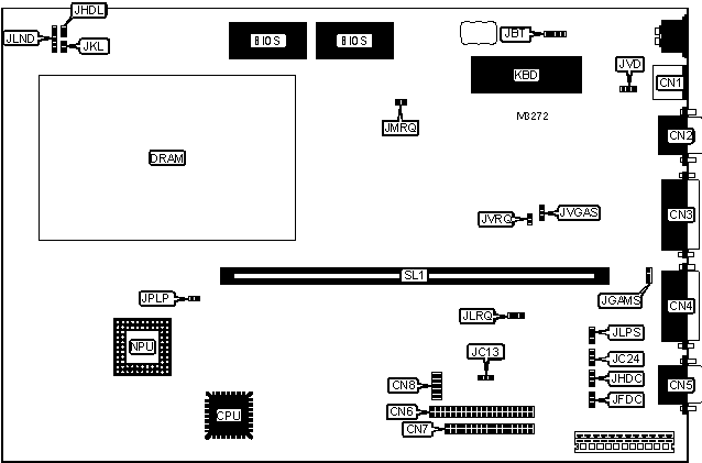
CONNECTIONS | |||
|
Function |
Label |
Function |
Label |
|
PS/2 mouse port |
CN1 |
Floppy drive interface |
CN7 |
|
VGA port |
CN2 |
Serial port 1 |
CN8 |
|
Game port |
CN3 |
External battery |
JBT |
|
Parallel port |
CN4 |
IDE interface LED |
JHDL |
|
Serial port 2 |
CN5 |
Front panel connector |
JLND |
|
IDE interface |
CN6 |
Riser slot |
SL1 |
|
USER CONFIGURABLE SETTINGS | |||
|
Setting |
Label |
Position | |
|
» |
Serial port 1 COM select COM1 |
JC13 |
Pins 1 & 2 closed |
|
Serial port 1 COM select COM3 |
JC13 |
Pins 2 & 3 closed | |
|
» |
Serial port 2 COM select COM2 |
JC24 |
Pins 1 & 2 closed |
|
Serial port 2 COM select COM4 |
JC24 |
Pins 2 & 3 closed | |
|
» |
Floppy drive interface enabled |
JFDC |
Pins 1 & 2 closed |
|
Floppy drive interface disabled |
JFDC |
Pins 2 & 3 closed | |
|
» |
Game port enabled |
JGAMS |
Pins 1 & 2 closed |
|
Game port disabled |
JGAMS |
Pins 2 & 3 closed | |
|
» |
IDE interface enabled |
JHDC |
Pins 1 & 2 closed |
|
IDE interface disabled |
JHDC |
Pins 2 & 3 closed | |
|
» |
Parallel port LPT select LPT1 |
JLPS |
Pins 1 & 2 closed |
|
Parallel port LPT select LPT2 |
JLPS |
Pins 2 & 3 closed | |
|
» |
Parallel port IRQ select IRQ7 |
JLRQ |
Pins 2 & 3 closed |
|
Parallel port IRQ select IRQ5 |
JLRQ |
Pins 1 & 2 closed | |
|
» |
Factory configured - do not alter |
JKL |
N/A |
|
» |
Mouse IRQ select IRQ12 |
JMRQ |
Closed |
|
Mouse IRQ select none |
JMRQ |
Open | |
|
» |
Pipeline mode enabled |
JPLP |
Closed |
|
Pipeline mode disabled |
JPLP |
Open | |
|
» |
Monitor type select color |
JVD |
Pins 2 & 3 closed |
|
Monitor type select monochrome |
JVD |
Pins 1 & 2 closed | |
|
» |
VGA IRQ select IRQ9 |
JVRQ |
Closed |
|
VGA IRQ select none |
JVRQ |
Open | |
|
» |
Onboard video enabled |
JVGAS |
Pins 1 & 2 closed |
|
Onboard video enabled |
JVGAS |
Pins 2 & 3 closed | |
|
DRAM | |||
|
Size |
Banks 0 & 1 |
Bank 2 |
Bank 3 |
|
1MB |
(8) 44256 & (4) 41256 |
None |
None |
|
2MB |
(8) 44256 & (4) 41256 |
(2) 256K x 9 |
(2) 256K x 9 |
|
3MB |
(8) 44256 & (4) 41256 |
(2) 1M x 9 |
None |
|
5MB |
(8) 44256 & (4) 41256 |
(2) 1M x 9 |
(2) 1M x 9 |
|
Note: Banks 0 & 1 are factory installed and not configurable. The orientation of the banks is unidentified. | |||
|
MISCELLANEOUS TECHNICAL NOTE |
|
The location of pin 1 is unidentified. |