PACKARD BELL
PB300/PB320 (REV. A)
|
Processor |
80386SX |
|
Processor Speed |
25MHz |
|
Chip Set |
ACC |
|
Max. onboard DRAM |
5MB |
|
Cache |
None |
|
BIOS |
Phoenix |
|
Dimensions |
230mm x 220mm |
|
I/O Options |
Fax/modem daughterboard, floppy drive interface, game port, IDE interface, parallel port, PS/2 keyboard port, PS/2 mouse port, serial port, VGA port |
|
NPU Options |
80387SX |
|
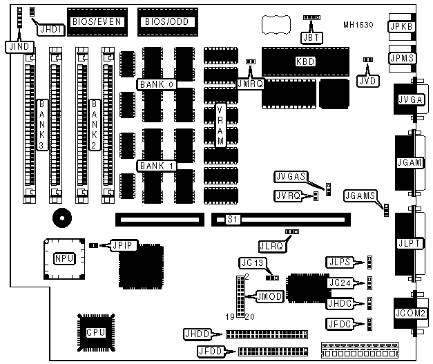
CONNECTIONS |
|||
|
Purpose |
Location |
Purpose |
Location |
|
External battery |
JBT |
Parallel port |
JLPT |
|
Serial port |
JCOM2 |
Proprietary modem daughterboard |
JMOD |
|
Floppy drive interface |
JFDD |
PS/2 keyboard |
JPKB |
|
Game port |
JGAM |
PS/2 mouse |
JPMS |
|
IDE interface |
JHDD |
VGA port |
JVGA |
|
IDE interface LED |
JHDI |
Riser card |
S1 |
|
Front panel connector |
JIND |
|
|
|
USER CONFIGURABLE SETTINGS |
|||
|
Function |
Jumper/Switch |
Position |
|
|
» |
Onboard floppy drive interface enabled |
JFDC |
pins 1 & 2 closed |
|
|
Onboard floppy drive interface disabled |
JFDC |
pins 2 & 3 closed |
|
» |
Onboard Game port disabled |
JGAMS |
pins 1 & 2 closed |
|
|
Onboard Game port enabled |
JGAMS |
pins 2 & 3 closed |
|
» |
Onboard IDE interface enabled |
JHDC |
pins 1 & 2 closed |
|
|
Onboard IDE interface disabled |
JHDC |
pins 2 & 3 closed |
|
» |
PS/2 mouse port enabled (IRQ12) |
JMRQ |
Closed |
|
|
PS/2 mouse port disabled |
JMRQ |
Open |
|
» |
Pipeline mode disabled |
JPIP |
Open |
|
|
Pipeline mode enabled |
JPIP |
Closed |
|
» |
Monitor type select color |
JVD |
pins 2 & 3 closed |
|
|
Monitor type select monochrome |
JVD |
pins 1 & 2 closed |
|
ONBOARD VIDEO CONFIGURATION |
||||
|
Onboard Video |
IRQ |
JVGAS |
JVRQ |
|
|
» |
Enabled |
IRQ9 |
pins 1 & 2 closed |
Closed |
|
|
Enabled |
None |
pins 1 & 2 closed |
Open |
|
|
Disabled |
N/A |
pins 2 & 3 closed |
N/A |
|
SERIAL PORT CONFIGURATION |
|||||
|
Modem (JMOD) |
Port B (JCOM2) |
ISA Modem |
JC13 |
JC24 |
JMOD |
|
Disabled |
COM2 |
None |
N/A |
pins 1 & 2 |
Closed |
|
Disabled |
COM2 |
COM1 |
pins 2 & 3 |
pins 1 & 2 |
Closed |
|
Disabled |
COM2 |
COM3 |
pins 1 & 2 |
pins 1 & 2 |
Closed |
|
COM1 |
COM2 |
None |
pins 1 & 2 |
pins 1 & 2 |
Daughterboard |
|
COM3 |
COM2 |
None |
pins 2 & 3 |
pins 1 & 2 |
Daughterboard |
|
Disabled |
COM4 |
None |
N/A |
pins 2 & 3 |
Closed |
|
Disabled |
COM4 |
COM1 |
pins 2 & 3 |
pins 2 & 3 |
Closed |
|
Disabled |
COM4 |
COM3 |
pins 1 & 2 |
pins 2 & 3 |
Closed |
|
COM1 |
COM4 |
None |
pins 1 & 2 |
pins 2 & 3 |
Daughterboard |
|
COM3 |
COM4 |
None |
pins 2 & 3 |
pins 2 & 3 |
Daughterboard |
|
Note: JMOD is closed using a special jumper, JMODJ, which connects pins 10 and 11. Permanent damage to the board will occur if the JMODJ jumper is installed improperly. Pins designated should be in the closed position. |
|||||
|
PARALLEL PORT CONFIGURATION |
||||
|
LPT |
IRQ |
JLPS |
JLRQ |
|
|
» |
LPT1 |
IRQ7 |
pins 1 & 2 closed |
pins 2 & 3 closed |
|
|
LPT1 |
IRQ5 |
pins 1 & 2 closed |
pins 1 & 2 closed |
|
|
LPT2 |
IRQ7 |
pins 2 & 3 closed |
pins 2 & 3 closed |
|
|
LPT2 |
IRQ5 |
pins 2 & 3 closed |
pins 1 & 2 closed |
|
DRAM CONFIGURATION |
||||
|
Size |
Bank 0 |
Bank 1 |
Bank 2 |
Bank 3 |
|
1MB |
(4) 44256 |
(4) 44256 |
NONE |
NONE |
|
3MB |
(4) 44256 |
(4) 44256 |
(2) 1M x 9 |
NONE |
|
5MB |
(4) 44256 |
(4) 44256 |
(2) 1M x 9 |
(2) 1M x 9 |
|
Note: Banks 0 & 1 are soldered to the board. |
||||