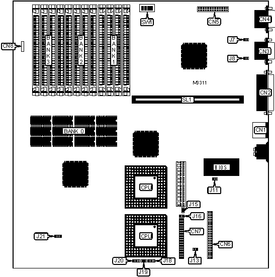
OLIVETTI
M400-40 (PCB BA301)
|
Processor |
80486SX/80487SX/80486DX |
|
Processor Speed |
25/33MHz |
|
Chip Set |
Unidentified |
|
Maximum Onboard Memory |
52MB |
|
Cache |
None |
|
BIOS |
Unidentified |
|
Dimensions |
355mm x 305mm |
|
I/O Options |
Floppy drive interface, IDE interface, parallel port, PS/2 mouse port, serial port, feature connector, VGA port, riser slot, console connector |
|
NPU Options |
None |
|
CONNECTIONS | |||
|
Function |
Label |
Function |
Label |
|
PS/2 mouse port |
CN1 |
IDE interface |
CN6 |
|
Parallel port |
CN2 |
Floppy drive interface |
CN7 |
|
Serial port |
CN3 |
Console connector |
CN8 |
|
VGA port |
CN4 |
Riser slot |
SL1 |
|
Feature connector |
CN5 | ||
|
USER CONFIGURABLE SETTINGS | |||
|
Setting |
Label |
Position | |
|
» |
ROM BIOS enabled |
J11 |
Closed |
|
ROM BIOS disabled |
J11 |
Open | |
|
» |
Floppy drive oscillator enabled |
J13 |
Closed |
|
Floppy drive oscillator disabled |
J13 |
Open | |
|
» |
CMOS memory normal operation |
J15 |
Open |
|
CMOS memory clear |
J15 |
Closed | |
|
» |
Hard drives installed 1 |
J16 |
Closed |
|
Hard drives installed 2 |
J16 |
Open | |
|
» |
Serial port enabled |
SW1/1 |
On |
|
Serial port disabled |
SW1/1 |
Off | |
|
» |
Factory configured - do not alter |
SW1/2 |
On |
|
» |
Floppy drive write enabled |
SW1/3 |
On |
|
Floppy drive write disabled |
SW1/3 |
Off | |
|
» |
Factory configured - do not alter |
SW1/4 |
On |
|
Note: The location of pin 1 on SW1 is unidentified. | |||
|
DRAM | ||||
|
Size |
Bank 0 |
Bank 1 |
Bank 2 |
Bank 3 |
|
4MB |
4MB |
None |
None |
None |
|
8MB |
4MB |
(4) 1M x 9 |
None |
None |
|
12MB |
4MB |
(4) 1M x 9 |
(4) 1M x 9 |
None |
|
16MB |
4MB |
(4) 1M x 9 |
(4) 1M x 9 |
(4) 1M x 9 |
|
20MB |
4MB |
(4) 4M x 9 |
None |
None |
|
24MB |
4MB |
(4) 1M x 9 |
(4) 4M x 9 |
None |
|
36MB |
4MB |
(4) 4M x 9 |
(4) 4M x 9 |
None |
|
40MB |
4MB |
(4) 1M x 9 |
(4) 4M x 9 |
(4) 4M x 9 |
|
40MB |
4MB |
(4) 4M x 9 |
(4) 4M x 9 |
(4) 1M x 9 |
|
40MB |
4MB |
(4) 4M x 9 |
(4) 1M x 9 |
(4) 4M x 9 |
|
52MB |
4MB |
(4) 4M x 9 |
(4) 4M x 9 |
(4) 4M x 9 |
|
Note: Bank 0 is factory installed and is not configurable. | ||||
|
CPU TYPE | |||
|
Setting |
J18 |
J19 |
J20 |
|
80486SX |
Open |
Open |
Pins 2 & 3 closed |
|
80487SX |
Pins 2 & 3 closed |
Closed |
Pins 1 & 2 closed |
|
80486DX |
Pins 1 & 2 closed |
Closed |
Pins 1 & 2 closed |
|
CPU SPEED | |
|
Setting |
J21 |
|
25MHz |
Pins 2 & 3 closed |
|
33MHz |
Pins 1 & 2 closed |
|
Note: The location of pin 1 is unidentified. | |
|
SERIAL PORT RING INDICATOR | |||
|
Setting |
J7 |
J8 | |
| » |
FAIL SAFE enabled (RS-232 threshold voltage) |
Closed |
Closed |
|
FAIL SAFE disabled(RS-232 threshold voltage) |
Open |
Open | |