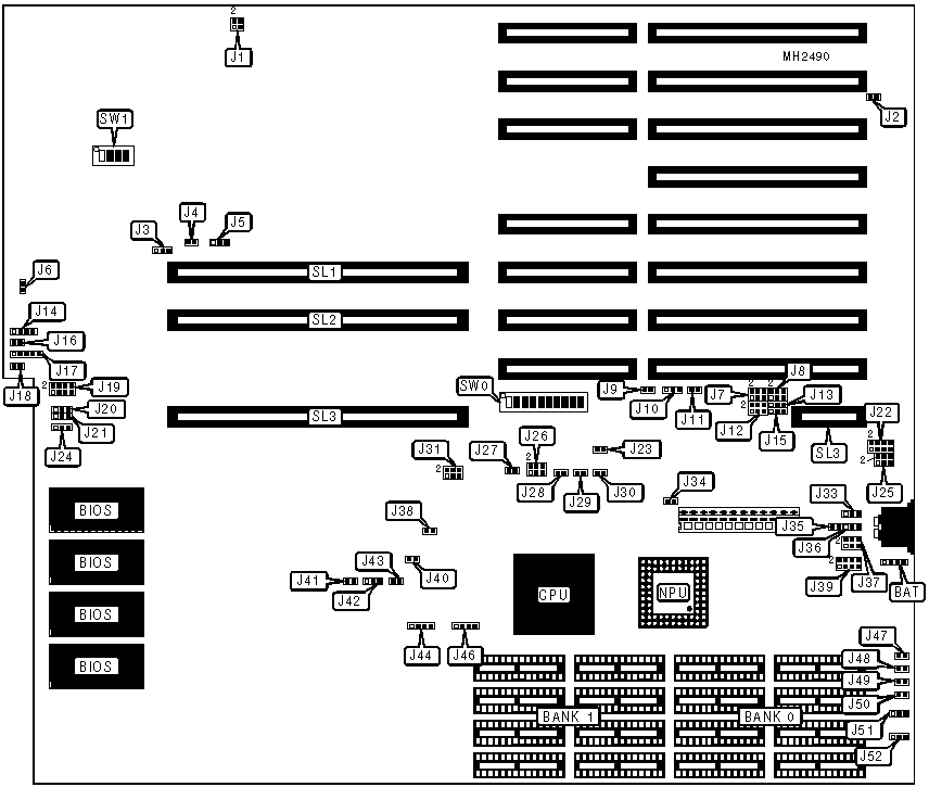
MYLEX CORPORATION
EM386X
|
Processor |
80386DX |
|
Processor Speed |
25/33MHz |
|
Chip Set |
Unidentified |
|
Max. Onboard DRAM |
32MB |
|
Cache |
16/32/64/128KB |
|
BIOS |
AMI/Award/Mylex/Phoenix |
|
Dimensions |
305mm x 330mm |
|
I/O Options |
32-bit Intel slots (2), 32-bit external memory card |
|
NPU Options |
80287/80387DX/3167 |
|
CONNECTIONS | |||
|
Purpose |
Location |
Purpose |
Location |
|
External battery |
BAT |
Power LED & keylock |
J17 |
|
Turbo switch |
J6 |
Reset switch |
J18 |
|
Single-step control switch |
J10 |
32-bit Intel slots |
SL1 & SL2 |
|
Speaker connector |
J14 |
32-bit external memory card |
SL3 |
|
Turbo LED |
J16 | ||
|
USER CONFIGURABLE SETTINGS | |||
|
Function |
Jumper |
Position | |
|
I/O bus speed select 1 wait states |
J1 |
Closed | |
|
I/O bus speed select 2 wait states |
J1 |
Open | |
|
» |
Factory configured - do not alter |
J2 |
Closed |
|
» |
Monitor type select monochrome |
J3 |
pins 1 & 2 closed |
|
Monitor type select color |
J3 |
pins 2 & 3 closed | |
|
» |
AT bus DRAM refresh signal disabled |
J4 |
Closed |
|
AT bus DRAM refresh signal enabled |
J4 |
Open | |
|
» |
80386 <Rev. D NPU interface bug bypass disabled |
J5 |
Open |
|
80386 <Rev. D NPU interface bug bypass enabled |
J5 |
Closed | |
|
» |
Turbo mode enabled |
J6 |
Open |
|
Turbo mode disabled |
J6 |
Closed | |
|
» |
Cache enabled |
J9 |
Open |
|
Cache disabled |
J9 |
Closed | |
|
» |
Factory configured - do not alter |
J11 |
N/A |
|
» |
Factory configured - do not alter |
J13 |
pins 1 & 2 closed |
|
» |
Factory configured - do not alter |
J15 |
pins 1 & 2 closed |
|
» |
Factory configured - do not alter |
J22 |
N/A |
|
» |
Factory configured - do not alter |
J23 |
Closed |
|
» |
Factory configured - do not alter |
J26 |
N/A |
|
» |
Factory configured - do not alter |
J27 |
Closed |
|
» |
Memory access on Intel 32-bit bus cached |
J28 |
Closed |
|
Memory access on Intel 32-bit bus cached |
J28 |
Open | |
|
» |
ROM address select 0F0000 and FF0000 |
J30 |
Open |
|
ROM address select 0F0000 |
J30 |
Closed | |
|
» |
Factory configured - do not alter |
J33 |
N/A |
|
» |
NPU type select 80387 |
J34 |
Closed |
|
NPU type select 80287 |
J34 |
Open | |
|
» |
NPU synchronous with CPU |
J35 |
Open |
|
NPU asynchronous with CPU |
J35 |
Closed | |
|
» |
Factory configured - do not alter |
J37 |
pins 1 & 2 closed |
|
» |
Factory configured - do not alter |
J38 |
N/A |
|
» |
80387 reset normal |
J40 |
Open |
|
80387 reset on port F1h |
J40 |
Closed | |
|
USER CONFIGURABLE SETTINGS (CON’T) | |||
|
Function |
Jumper/Switch |
Position | |
|
» |
ROM caching disabled |
J41 |
Open |
|
ROM caching enabled |
J41 |
Closed | |
|
» |
Single step mode disabled |
J42 |
pins 2 & 3 closed |
|
Single step mode enabled |
J42 |
pins 1 & 2 closed | |
|
» |
Factory configured - do not alter |
J43 |
N/A |
|
» |
BIOS speed select 250ns |
J44 |
pins 3 & 4 closed |
|
BIOS speed select 200ns |
J44 |
pins 1 & 2 closed | |
|
BIOS speed select 200ns for 25MHz machine |
J44 |
Open | |
|
BIOS speed select 150ns for 33MHz machine |
J44 |
Open | |
|
» |
Factory configured - do not alter |
J46 |
N/A |
|
» |
Factory configured - do not alter |
J47 |
N/A |
|
» |
Factory configured - do not alter |
J48 |
N/A |
|
» |
Factory configured - do not alter |
J49 |
N/A |
|
» |
Factory configured - do not alter |
J50 |
N/A |
|
» |
Intel NPU not installed |
SW0/1 |
On |
|
Intel NPU installed |
SW0/1 |
Off | |
|
» |
No ISA bus card installed w/memory between 12 and 14MB |
SW0/2 |
On |
|
ISA bus card installed with memory between 12 and 14MB |
SW0/2 |
Off | |
|
ROM shadowing disabled |
SW0/8 |
On | |
|
ROM shadowing enabled |
SW0/8 |
Off | |
|
» |
Factory configured - do not alter |
SW0/9 |
N/A |
|
» |
Factory configured - do not alter |
SW0/10 |
N/A |
|
CACHE CONFIGURATION | |||
|
Size |
Bank 0 |
Bank 1 |
TAG |
|
16KB |
(8) 4K x 4 |
NONE |
(>1) 4K x 4 |
|
32KB 1 |
(8) 4K x 4 |
(8) 4K x 4 |
(>1) 16K x 4 |
|
32KB 2 |
(8) 8K x 4 |
NONE |
(>1) 16K x 4 |
|
64KB |
(8) 16K x 4 |
NONE |
(>1) 16K x 4 |
|
128KB |
(8) 16K x 4 |
(8) 16K x 4 |
(>1) 16K x 4 |
|
Note: The exact location and number of tag chips is unidentified. | |||
|
CACHE JUMPER CONFIGURATION | |||||
|
Size |
J7 |
J8 |
J12 |
J29 |
J31 |
|
16KB |
pins 5 & 6 closed |
pins 3 & 4 closed |
pins 5 & 6 closed |
Open |
pins 1 & 2 closed |
|
32KB 1 |
pins 5 & 6 closed |
pins 5 & 6 closed |
pins 5 & 6 closed |
Closed |
pins 5 & 6 closed |
|
32KB 2 |
pins 5 & 6 closed |
pins 5 & 6 closed |
pins 5 & 6 closed |
Open |
pins 1 & 2 closed |
|
64KB |
pins 5 & 6 closed |
pins 5 & 6 closed |
pins 3 & 4 closed |
Open |
pins 1 & 2 closed |
|
128KB |
pins 3 & 4 closed |
pins 5 & 6 closed |
pins 3 & 4 closed |
Closed |
pins 3 & 4 closed |
|
CACHE JUMPER CONFIGURATION (CON’T) | ||||
|
Size |
J36 |
J39 |
J51 |
J52 |
|
16KB |
pins 2 & 3 closed |
pins 5 & 6 closed |
pins 2 & 3 closed |
pins 2 & 3 closed |
|
32KB 1 |
pins 2 & 3 closed |
pins 7 & 8 closed |
pins 2 & 3 closed |
pins 2 & 3 closed |
|
32KB 2 |
pins 2 & 3 closed |
pins 5 & 6 closed |
pins 2 & 3 closed |
pins 2 & 3 closed |
|
64KB |
pins 1 & 2 closed |
pins 5 & 6 closed |
pins 1 & 2 closed |
pins 1 & 2 closed |
|
128KB |
pins 1 & 2 closed |
pins 3 & 4 closed |
pins 1 & 2 closed |
pins 1 & 2 closed |
|
DRAM CONFIGURATION | ||
|
Size |
Bank 0 |
Bank 1 |
|
1MB |
(4) 256K x 9 |
NONE |
|
2MB |
(4) 256K x 9 |
(4) 256K x 9 |
|
4MB |
(4) 1M x 9 |
NONE |
|
8MB |
(4) 1M x 9 |
(4) 1M x 9 |
|
16MB |
(4) 4M x 9 |
NONE |
|
32MB |
(4) 4M x 9 |
(4) 4M x 9 |
|
DRAM SWITCH CONFIGURATION | |||||
|
Size |
EMS Size |
SW1/1 |
SW1/2 |
SW1/3 |
SW1/4 |
|
1MB |
NONE |
On |
On |
On |
On |
|
1MB |
0.375MB |
Off |
On |
On |
On |
|
2MB |
1MB |
On |
On |
Off |
On |
|
2MB |
1.375MB |
Off |
On |
Off |
On |
|
4MB |
3MB |
On |
On |
Off |
Off |
|
4MB |
3.375MB |
Off |
On |
Off |
Off |
|
8MB |
7MB |
Off |
On |
Off |
Off |
|
8MB |
7.375MB |
On |
Off |
On |
On |
|
16MB |
13MB |
On |
Off |
On |
Off |
|
16MB |
14.875MB |
On |
Off |
Off |
On |
|
32MB |
30.875MB |
On |
Off |
Off |
Off |
|
DRAM SPEED CONFIGURATION | |||||
|
CPU Speed |
DRAM Speed |
J25 |
SW0/5 |
SW0/6 |
SW0/7 |
|
25MHz |
80ns |
pins 1 & 2 closed |
On |
On |
On |
|
25MHz |
100ns |
pins 3 & 4 closed |
Off |
Off |
Off |
|
33MHz |
60ns |
pins 1 & 2 closed |
On |
On |
On |
|
33MHz |
80ns |
pins 3 & 4 closed |
Off |
Off |
Off |
|
BIOS TYPE CONFIGURATION | |||
|
» Type |
J21 |
J24 | |
| » |
27256 |
pins 1 & 2 closed |
pins 2 & 3 closed |
| » |
27128 |
pins 1 & 2 closed |
pins 1 & 2 closed |
| » |
27512 |
pins 2 & 3 closed |
pins 2 & 3 closed |
|
CACHEABLE AREA SELECTION | ||||
|
Cacheable RAM |
Min. cache size |
SW0/2 |
SW0/3 |
SW0/4 |
|
32MB |
128KB |
N/A |
Off |
Off |
|
16MB |
64KB |
N/A |
On |
Off |
|
14MB |
128KB |
Off |
Off |
On |
|
8MB |
128KB |
On |
Off |
On |
|
4MB |
N/A |
N/A |
On |
On |
|
DRAM/CACHE MODE CONFIGURATION | ||||||
|
DRAM size |
Interleave |
Cache size |
J19 |
J20 |
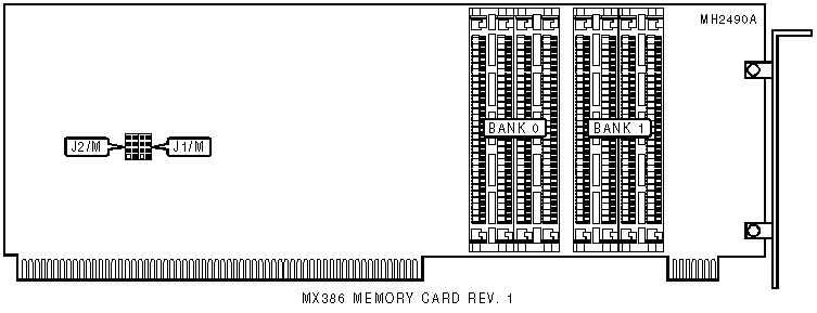
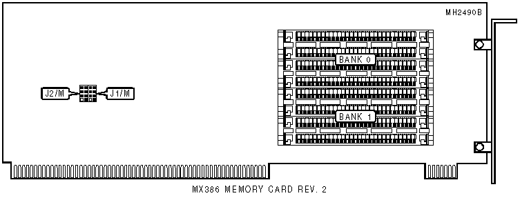
J1/M |
J2/M |
|
1MB |
No |
Any |
Open |
2 & 3 |
1 & 2 |
1 & 2 |
|
2MB |
No |
Any |
3 & 4 |
Open |
1 & 2 |
1 & 2 |
|
2MB |
Yes |
16KB |
Open |
1 & 2 |
1 & 2 |
3 & 4 |
|
2MB |
Yes |
32KB 1 |
1 & 2 |
Open |
3 & 4 |
1 & 2 |
|
2MB |
Yes |
32KB 2 |
Open |
1 & 2 |
1 & 2 |
3 & 4 |
|
2MB |
Yes |
64KB |
Open |
1 & 2 |
1 & 2 |
3 & 4 |
|
2MB |
Yes |
128KB |
1 & 2 |
Open |
3 & 4 |
1 & 2 |
|
4MB |
No |
Any |
Open |
2 & 3 |
1 & 2 |
1 & 2 |
|
8MB |
No |
Any |
5 & 6 |
Open |
1 & 2 |
1 & 2 |
|
8MB |
Yes |
16KB |
Open |
1 & 2 |
1 & 2 |
5 & 6 |
|
8MB |
Yes |
32KB 1 |
1 & 2 |
Open |
5 & 6 |
1 & 2 |
|
8MB |
Yes |
32KB 2 |
Open |
1 & 2 |
1 & 2 |
5 & 6 |
|
8MB |
Yes |
64KB |
Open |
1 & 2 |
1 & 2 |
5 & 6 |
|
8MB |
Yes |
128KB |
1 & 2 |
Open |
5 & 6 |
1 & 2 |
|
16MB |
No |
Any |
Open |
2 & 3 |
1 & 2 |
1 & 2 |
|
32MB |
No |
Any |
7 & 8 |
Open |
1 & 2 |
1 & 2 |
|
32MB |
Yes |
16KB |
Open |
1 & 2 |
1 & 2 |
7 & 8 |
|
32MB |
Yes |
32KB 1 |
1 & 2 |
Open |
7 & 8 |
1 & 2 |
|
32MB |
Yes |
32KB 2 |
Open |
1 & 2 |
1 & 2 |
7 & 8 |
|
32MB |
Yes |
64KB |
Open |
1 & 2 |
1 & 2 |
7 & 8 |
|
32MB |
Yes |
128KB |
1 & 2 |
Open |
7 & 8 |
1 & 2 |
|
Note: Pins designated should be in the closed position. | ||||||