INTEL CORPORATION
CU430HX
|
Processor |
Pentium |
|
Processor Speed |
75/90/100/120/133/150/166/200MHz |
|
Chip Set |
Intel |
|
Video Chip Set |
ATI |
|
Maximum Onboard Memory |
192MB (EDO supported) |
|
Maximum Video Memory |
4MB |
|
Cache |
256/512KB |
|
BIOS |
Unidentified |
|
Dimensions |
300mm x 210mm |
|
I/O Options |
Floppy drive interface, green PC connector, IDE interfaces (2), parallel port, PS/2 mouse port, serial ports (3), VGA header connector, VGA port, riser slot, cache slot, IR connector, USB connector, LAN connector, microphone port, audio output port, CD audio connector, modem connector, wave table connector, MIDI/audio interface |
|
NPU Options |
None |
|
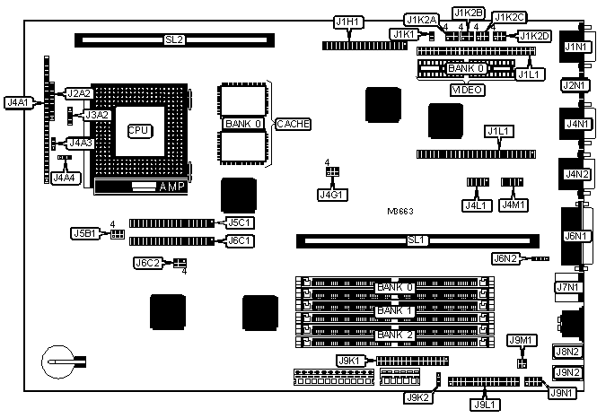
CONNECTIONS | |||
|
Purpose |
Location |
Purpose |
Location |
|
Security connector |
J1K1 |
Serial port 2 |
J4M1 |
|
VGA header connector |
J1H1 |
USB connector |
J4N1 |
|
VGA port |
J1N1 |
Serial port 3 |
J4N2 |
|
Front panel connector |
J2A2 |
IDE interface 1 |
J5C1 |
|
LAN connector |
J2N1 |
IDE interface 2 |
J6C1 |
|
Power LED/IDE interface LED |
J3A2 |
Parallel port |
J6N1 |
|
Chassis fan power |
J4A1 pins 1 - 3 |
CD audio connector |
J6N2 |
|
Reset switch |
J4A1 pins 4 & 5 |
PS/2 mouse port |
J7N1 |
|
Power LED |
J4A1 pins 7 - 10 |
Microphone port |
J8N2 |
|
IDE interface LED |
J4A1 pins 11 - 14 |
Floppy drive interface |
J9K1 |
|
Power supply on connector |
J4A1 pins 15 & 16 |
MIDI/audio interface |
J9L1 |
|
Green PC connector |
J4A1 pins 17 & 18 |
Modem connector |
J9M1 |
|
IR connector |
J4A1 pins 20 - 25 |
Wave table connector |
J9N1 |
|
Speaker |
J4A1 pins 26 - 29 |
Audio output port |
J9N2 |
|
Keylock |
J4A3 |
Riser slot |
SL1 |
|
Chassis fan power |
J4A4 |
Cache slot |
SL2 |
|
Serial port 1 |
J4L1 | ||
|
USER CONFIGURABLE SETTINGS | |||
|
Function |
Label |
Position | |
|
» |
Password normal operation |
J1K2A |
Pins 1 & 2 closed |
|
Password clear |
J1K2A |
Pins 2 & 3 closed | |
|
» |
CMOS memory normal operation |
J1K2A |
Pins 4 & 5 closed |
|
CMOS memory clear |
J1K2A |
Pins 5 & 6 closed | |
|
» |
Setup access enabled |
J1K2B |
Pins 1 & 2 closed |
|
Setup access disabled |
J1K2B |
Pins 2 & 3 closed | |
|
» |
Factory configured - do not alter |
J1K2B |
Pins 5 & 6 closed |
|
» |
2 PCI slots on riser card |
J4G1 |
Pins 1 & 2, 4 & 5 closed |
|
3 PCI slots on riser card |
J4G1 |
Pins 2 & 3, 5 & 6 closed | |
|
» |
Flash BIOS normal operation |
J6C2 |
Pins 1 & 2 closed |
|
Flash BIOS recovery mode |
J6C2 |
Pins 2 & 3 closed | |
|
DRAM CONFIGURATION | |||
|
Size |
Bank 0 |
Bank 1 |
Bank 2 |
|
16MB |
(2) 1M x 36 |
(2) 1M x 36 |
None |
|
16MB |
(2) 2M x 36 |
None |
None |
|
24MB |
(2) 2M x 36 |
(2) 1M x 36 |
None |
|
24MB |
(2) 1M x 36 |
(2) 1M x 36 |
(2) 1M x 36 |
|
32MB |
(2) 4M x 36 |
None |
None |
|
32MB |
(2) 2M x 36 |
(2) 2M x 36 |
None |
|
40MB |
(2) 4M x 36 |
(2) 1M x 36 |
None |
|
48MB |
(2) 4M x 36 |
(2) 2M x 36 |
None |
|
DRAM CONFIGURATION (CON’T) | |||
|
Size |
Bank 0 |
Bank 1 |
Bank 2 |
|
48MB |
(2) 4M x 36 |
(2) 1M x 36 |
(2) 1M x 36 |
|
64MB |
(2) 8M x 36 |
None |
None |
|
64MB |
(2) 4M x 36 |
(2) 4M x 36 |
None |
|
80MB |
(2) 8M x 36 |
(2) 2M x 36 |
None |
|
80MB |
(2) 8M x 36 |
(2) 1M x 36 |
(2) 1M x 36 |
|
88MB |
(2) 8M x 36 |
(2) 2M x 36 |
(2) 1M x 36 |
|
96MB |
(2) 8M x 36 |
(2) 4M x 36 |
None |
|
96MB |
(2) 4M x 36 |
(2) 4M x 36 |
(2) 4M x 36 |
|
96MB |
(2) 8M x 36 |
(2) 2M x 36 |
(2) 2M x 36 |
|
104MB |
(2) 8M x 36 |
(2) 4M x 36 |
(2) 1M x 36 |
|
112MB |
(2) 8M x 36 |
(2) 4M x 36 |
(2) 2M x 36 |
|
128MB |
(2) 8M x 36 |
(2) 4M x 36 |
(2) 4M x 36 |
|
128MB |
(2) 8M x 36 |
(2) 8M x 36 |
None |
|
136MB |
(2) 8M x 36 |
(2) 8M x 36 |
(2) 1M x 36 |
|
144MB |
(2) 8M x 36 |
(2) 8M x 36 |
(2) 2M x 36 |
|
160MB |
(2) 16M x 36 |
(2) 4M x 36 |
None |
|
192MB |
(2) 8M x 36 |
(2) 8M x 36 |
(2) 8M x 36 |
|
Note: Board accepts EDO memory. Board also accepts x 32 SIMMs. | |||
|
CACHE CONFIGURATION | ||
|
Size |
Bank 0 |
SL1 |
|
256KB |
(2) 32K x 32 |
None |
|
512KB |
(2) 32K x 32 |
256KB module installed |
|
VIDEO MEMORY CONFIGURATION | ||
|
Size |
Bank 0 |
J1L1 |
|
1MB |
(2) 128K x 32 |
None |
|
4MB |
(2) 128K x 32 |
Module installed |
|
Note: Module is inserted in both connectors labeled J1L1. | ||
|
CPU SPEED SELECTION | ||||
|
CPU speed |
Clock speed |
Multiplier |
J1K2C |
J1K2D |
|
75MHz |
50MHz |
1.5x |
2 & 3, 5 & 6 |
1 & 2, 4 & 5 |
|
90MHz |
60MHz |
1.5x |
2 & 3, 4 & 5 |
1 & 2, 4 & 5 |
|
100MHz |
66MHz |
1.5x |
1 & 2, 5 & 6 |
1 & 2, 4 & 5 |
|
120MHz |
60MHz |
2x |
2 & 3, 4 & 5 |
2 & 3, 4 & 5 |
|
133MHz |
66MHz |
2x |
1 & 2, 5 & 6 |
2 & 3, 4 & 5 |
|
150MHz |
60MHz |
2.5x |
2 & 3, 4 & 5 |
2 & 3, 5 & 6 |
|
166MHz |
66MHz |
2.5x |
1 & 2, 5 & 6 |
2 & 3, 5 & 6 |
|
200MHz |
66MHz |
3x |
1 & 2, 5 & 6 |
1 & 2, 5 & 6 |
|
Note: Pins designated should be in the closed position. | ||||
|
CPU TYPE SELECTION | |
|
Type |
J6C2 |
|
VR |
Pins 4 & 5 closed |
|
VRE |
Pins 5 & 6 closed |
|
VCC2 SELECTION | |
|
Setting |
J5B1 |
|
VCC2 not connected |
Open |
|
VCC2 connected (processors using MMX technology) |
Pins 1 & 4, 2 & 5, 3 & 6 closed |