KT TECHNOLOGY PTE LTD.
KT333OP3C-WB/BI PQFP 386DX MAINBOARD
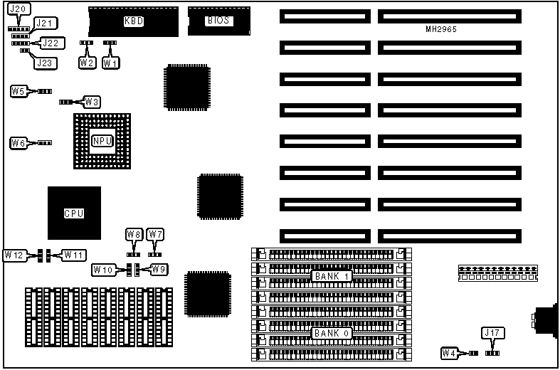
|
Processor |
80386DX |
|
Processor Speed |
25/33/40MHz |
|
Chip Set |
VLSI |
|
Max. Onboard DRAM |
32MB |
|
Cache |
32/64/128/256KB |
|
BIOS |
AMI |
|
Dimensions |
330mm x 218mm |
|
I/O Options |
None |
|
NPU Options |
80387DX/3167 |
|
CONNECTIONS | |||
|
Purpose |
Location |
Purpose |
Location |
|
External battery |
J17 |
Turbo LED & turbo switch |
J22 |
|
Power LED & keylock |
J20 |
Reset switch |
J23 |
|
Speaker |
J21 | ||
|
USER CONFIGURABLE SETTINGS | |||
|
Function |
Jumper |
Position | |
|
» |
Normal operation |
W1 |
Open |
|
Manufacturer testing |
W1 |
Closed | |
|
» |
Monitor type select color |
W2 |
pins 1 & 2 closed |
|
Monitor type select monochrome |
W2 |
pins 2 & 3 closed | |
|
» |
Bus clock speed select 4 |
W3 |
pins 1 & 2 closed |
|
Bus clock speed select 3 |
W3 |
pins 2 & 3 closed | |
|
» |
Factory configured - do not alter |
W4 |
N/A |
|
» |
CMOS memory normal operation |
W5 |
pins 1 & 2 closed |
|
CMOS memory clear |
W5 |
pins 2 & 3 closed | |
|
» |
NPU input clock select external oscillation for 80387 |
W6 |
pins 1 & 2 closed |
|
NPU input clock select internal oscillation for 80386 |
W6 |
pins 2 & 3 closed | |
|
DRAM CONFIGURATION | ||
|
Size |
Bank 0 |
Bank 1 |
|
1MB |
(4) 256K x 9 |
NONE |
|
2MB |
(4) 256K x 9 |
(4) 256K x 9 |
|
4MB |
(4) 1M x 9 |
NONE |
|
5MB |
(4) 256K x 9 |
(4) 1M x 9 |
|
8MB |
(4) 1M x 9 |
(4) 1M x 9 |
|
16MB |
(4) 4M x 9 |
NONE |
|
20MB |
(4) 1M x 9 |
(4) 4M x 9 |
|
20MB |
(4) 4M x 9 |
(4) 1M x 9 |
|
32MB |
(4) 4M x 9 |
(4) 4M x 9 |
|
CACHE CONFIGURATION | |||
|
Size |
Bank 0 |
Bank 1 |
TAG |
|
32KB |
(4) 8K x 8 |
NONE |
(3) 4K x 4 |
|
64KB |
(4) 8K x 8 |
(4) 8K x 8 |
(3) 4K x 4 |
|
128KB |
(4) 32K x 8 |
NONE |
(3) 16K x 4 |
|
256KB |
(4) 32K x 8 |
(4) 32K x 8 |
(3) 16K x 4 |
|
Note: The location of Bank 0 and Bank 1 are unidentified. The location of the Tag is unidentified. | |||
|
CACHE JUMPER CONFIGURATION | ||||||
|
Size |
W7 |
W8 |
W9 |
W10 |
W11 |
W12 |
|
32KB |
1 & 2 |
1 & 2 |
1 & 2 |
1 & 2 |
1 & 2 |
1 & 2 |
|
64KB |
1 & 2 |
1 & 2 |
1 & 2 |
1 & 2 |
2 & 3 |
2 & 3 |
|
128KB |
2 & 3 |
2 & 3 |
1 & 2 |
1 & 2 |
2 & 3 |
2 & 3 |
|
256KB |
2 & 3 |
2 & 3 |
2 & 3 |
2 & 3 |
2 & 3 |
2 & 3 |