EVEREX SYSTEMS, INC.
STEP 386 REV. E
|
Processor |
80386DX |
|
Processor Speed |
16/20MHz |
|
Chip Set |
C & T |
|
Max. Onboard DRAM |
8MB |
|
Cache |
64/128KB |
|
BIOS |
AMI |
|
Dimensions |
355mm x 304mm |
|
I/O Options |
32-bit proprietary memory card |
|
NPU Options |
80387DX |
|
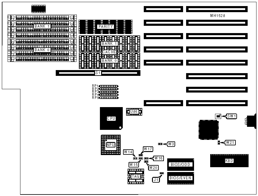
CONNECTIONS | |
|
Purpose |
Location |
|
32-bit proprietary memory card |
S1 |
|
USER CONFIGURABLE SETTINGS | |||
|
Function |
Jumper/Switch |
Position | |
| » |
Factory configured - do not alter |
J1 |
Unknown |
| » |
Factory configured - do not alter |
SW1 |
Unknown |
| » |
NPU enabled |
W3 |
Closed |
|
NPU disabled |
W3 |
Open | |
| » |
32-bit memory card enabled |
W14 |
Closed |
|
32-bit memory card disabled |
W14 |
Open | |
| » |
Base memory select 640KB |
W16 |
Closed |
|
Base memory select 512KB |
W16 |
Open | |
| » |
Bus speed select 10MHz |
W17 |
Closed |
|
Bus speed select 6.7MHz |
W17 |
Open | |
| » |
Parity enabled |
W20 |
Closed |
|
Parity disabled |
W20 |
Open | |
| » |
System memory select 2 banks enabled |
W21 |
Closed |
|
System memory select 1 bank enabled |
W21 |
Open | |
|
DRAM CONFIGURATION | ||||||
|
Size |
Bank 0 |
Bank 1 |
Bank 2 |
Bank 3 |
W1 |
W15 |
|
1MB |
(4) 256K x 9 |
NONE |
NONE |
NONE |
Closed |
Closed |
|
2MB |
(4) 256K x 9 |
(4) 256K x 9 |
NONE |
NONE |
Closed |
Closed |
|
4MB |
(4) 1M x 9 |
NONE |
NONE |
NONE |
Open |
Open |
|
4MB |
(4) 256K x 9 |
(4) 256K x 9 |
(4) 256K x 9 |
(4) 256K x 9 |
Closed |
Closed |
|
8MB |
(4) 1M x 9 |
(4) 1M x 9 |
NONE |
NONE |
Open |
Open |
|
16MB |
(4) 1M x 9 |
(4) 1M x 9 |
(4) 1M x 9 |
(4) 1M x 9 |
Open |
Open |
|
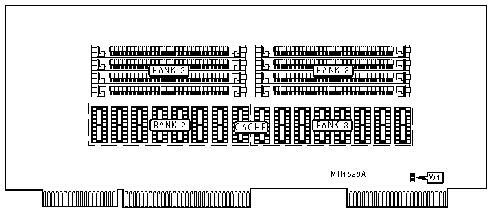
Note:Banks 2 & 3, and W1 are located on the external memory Board. | ||||||
|
CACHE CONFIGURATION | ||||
|
Size |
Cache |
Location |
TAG |
Dirty Bit (U38) |
|
64KB |
(8) 16K x 4 |
Bank 0 |
(2) 16K x 4 |
(1) 16K x 4 |
|
128KB |
(8) 16K x 4 |
Bank 0 & 1 |
(2) 16K x 4 |
(1) 16K x 4 |
|
Note:Each CACHE bank must be fully populated when its corresponding DRAM bank is populated. | ||||
|
RESISTOR SIPS CONFIGURATION | |
|
Settings |
Memory Banks enabled |
|
RP27, RP30, RP58, & RP61 installed |
Bank 0 |
|
RP28, RP31, RP59, & RP62 installed |
Bank 0 & 1 |
|
RP29, RP32, RP60, & RP63 installed |
Banks 0, 1, 2, & 3 |
|
CACHE CONFIGURATION | ||
|
Size |
Cache |
Location |
|
64KB |
(8) 16K x 4 |
Bank 2 |
|
128KB |
(8) 16K x 4 |
Bank 2 & 3 |
|
Note:Each CACHE bank must be fully populated when its corresponding DRAM bank is populated. | ||