HYUNDAI ELECTRONICS, INC.
CORPORATE SERIES 386/486 (VER. E & LATER)
|
Processor |
80386DX/80486SX/80486DX |
|
Processor Speed |
20/25/33/40/50MHz |
|
Chip Set |
Northport/VLSI |
|
Max. Onboard DRAM |
64MB |
|
Cache |
64/256KB (on CPU card) |
|
BIOS |
AMI |
|
Dimensions |
355.6mm x 304.8mm |
|
I/O Options |
Serial ports (2), parallel port, floppy drive interface, IDE interface, proprietary CPU card slot |
|
NPU Options |
80387/3167/4167 |
|
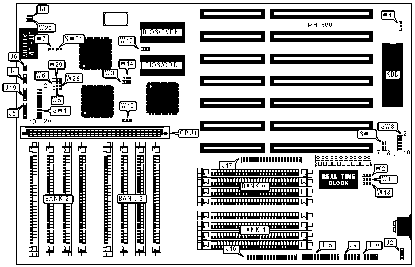
CONNECTIONS |
|||
|
Purpose |
Location |
Purpose |
Location |
|
Proprietary CPU card |
CPU1 |
Serial port 1 |
J9 |
|
External battery |
J2 |
Serial port 2 |
J10 |
|
Turbo LED |
J4 |
Parallel port |
J15 |
|
Power LED & keylock |
J5 |
Floppy drive interface |
J16 |
|
Reset switch |
J6 |
IDE interface |
J17 |
|
IDE interface LED |
J8 |
Speaker |
J19 |
|
Note: Although the CPU card supports a 50MHz processor, only a 40MHz 386DX, a 20MHz 486SX, and a 33MHz 486DX version are sold by Hyundai. |
|||
|
USER CONFIGURABLE SETTINGS |
|||
|
Function |
Jumper/Switch |
Position |
|
|
» |
Factory configured - do not alter |
SW1 pins 1 & 2 |
Open |
|
» |
Factory configured - do not alter |
SW1 pins 3 & 4 |
Closed |
|
» |
Factory configured - do not alter |
SW1 pins 5 & 6 |
Closed |
|
» |
Video BIOS shadowing enabled |
SW1 pins 7 & 8 |
Closed |
|
|
Video BIOS shadowing disabled |
SW1 pins 7 & 8 |
Open |
|
» |
SCSI BIOS shadowing disabled |
SW1 pins 9 & 10 |
Open |
|
|
SCSI BIOS shadowing enabled |
SW1 pins 9 & 10 |
Closed |
|
» |
ROM BIOS shadowing enabled |
SW1 pins 11 & 12 |
Closed |
|
|
ROM BIOS shadowing disabled |
SW1 pins 11 & 12 |
Open |
|
» |
Serial port 2 interrupt select IRQ3 |
SW2 pins 1 & 2 |
Closed |
|
|
Serial port 2 interrupt select none |
SW2 pins 1 & 2 |
Open |
|
» |
Serial port 1 interrupt select IRQ4 |
SW2 pins 3 & 4 |
Closed |
|
|
Serial port 1 interrupt select none |
SW2 pins 3 & 4 |
Open |
|
» |
Floppy drive interface enabled |
SW3 pins 1 & 2 |
Open |
|
|
Floppy drive interface enabled |
SW3 pins 1 & 2 |
Closed |
|
» |
Serial port 2 select COM2/2F8h |
SW3 pins 3 & 4 |
Open |
|
|
Serial port 2 disabled |
SW3 pins 3 & 4 |
Closed |
|
» |
Serial port 1 select COM1/3F8h |
SW3 pins 5 & 6 |
Open |
|
|
Serial port 1 disabled |
SW3 pins 5 & 6 |
Closed |
|
» |
BIOS cache location select 486DX internal cache |
SW4/3 |
On |
|
|
BIOS cache location select external cache |
SW4/3 |
Off |
|
» |
BIOS (E000-EFFFh) shadowing enabled |
SW4/4 |
On |
|
|
BIOS (E000-EFFFh) shadowing disabled |
SW4/4 |
Off |
|
» |
DRAM transparent refresh enabled |
SW4/5 |
On |
|
|
DRAM transparent refresh disabled |
SW4/5 |
Off |
|
» |
Factory configured - do not alter |
SW5/1 |
Off |
|
» |
Factory configured - do not alter |
SW5/2 |
On |
|
» |
IDE interface interrupt select IRQ14 |
SW21 |
On |
|
|
IDE interface interrupt select none |
SW21 |
Off |
|
» |
Floppy drive precompensation select standard |
W2 |
pins 2 & 3 closed |
|
|
Floppy drive precompensation select alternate |
W2 |
pins 1 & 2 closed |
|
» |
CPU speed select fast/switchable from keyboard |
W3 |
pins 2 & 3 closed |
|
|
CPU speed select fast |
W3 |
Open |
|
|
CPU speed select slow |
W3 |
pins 1 & 2 closed |
|
» |
Monitor type select color |
W4 |
pins 2 & 3 closed |
|
|
Monitor type select monochrome |
W4 |
pins 1 & 2 closed |
|
» |
CMOS memory normal operation |
W7 |
Open |
|
|
CMOS memory clear |
W7 |
Closed |
|
» |
Parallel port mode select bi-directional |
W13 |
pins 2 & 3 closed |
|
|
Parallel port mode select input only |
W13 |
pins 1 & 2 closed |
|
» |
Floppy drive type select single-speed |
W18 |
pins 1 & 2 closed |
|
|
Floppy drive type select dual-speed |
W18 |
pins 2 & 3 closed |
|
USER CONFIGURABLE SETTINGS (CON'T) |
|||
|
Function |
Jumper/Switch |
Position |
|
|
» |
BIOS type select 27256 |
W19 |
pins 2 & 3 closed |
|
|
BIOS type select 27512 |
W19 |
pins 1 & 2 closed |
|
» |
IDE interface enabled |
W20 |
Open |
|
|
IDE interface disabled |
W20 |
Closed |
|
Note: The locations of SW4 & SW5 are unidentified. |
|||
|
DRAM CONFIGURATION |
||||
|
Size |
Bank 0 |
Bank 1 |
Bank 2 |
Bank 3 |
|
1MB |
(4) 256K x 9 |
NONE |
NONE |
NONE |
|
2MB |
(4) 256K x 9 |
(4) 256K x 9 |
NONE |
NONE |
|
4MB |
(4) 1M x 9 |
NONE |
NONE |
NONE |
|
6MB |
(4) 256K x 9 |
(4) 256K x 9 |
(4) 1M x 9 |
NONE |
|
8MB |
(4) 1M x 9 |
(4) 1M x 9 |
NONE |
NONE |
|
10MB |
(4) 256K x 9 |
(4) 256K x 9 |
(4) 1M x 9 |
(4) 1M x 9 |
|
12MB |
(4) 1M x 9 |
(4) 1M x 9 |
(4) 1M x 9 |
NONE |
|
16MB |
(4) 1M x 9 |
(4) 1M x 9 |
(4) 1M x 9 |
(4) 1M x 9 |
|
16MB |
(4) 4M x 9 |
NONE |
NONE |
NONE |
|
24MB |
(4) 1M x 9 |
(4) 1M x 9 |
(4) 4M x 9 |
NONE |
|
32MB |
(4) 4M x 9 |
(4) 4M x 9 |
NONE |
NONE |
|
36MB |
(4) 1M x 9 |
(4) 4M x 9 |
(4) 4M x 9 |
NONE |
|
40MB |
(4) 1M x 9 |
(4) 1M x 9 |
(4) 4M x 9 |
(4) 4M x 9 |
|
48MB |
(4) 4M x 9 |
(4) 4M x 9 |
(4) 4M x 9 |
NONE |
|
64MB |
(4) 4M x 9 |
(4) 4M x 9 |
(4) 4M x 9 |
(4) 4M x 9 |
|
DRAM JUMPER CONFIGURATION |
|||||
|
Size |
SW1 |
W5 |
W6 |
W28 |
W29 |
|
1MB |
13 & 14, 15 & 16, 17 & 18, 19 & 20 |
2 & 3 |
2 & 3 |
Open |
Open |
|
2MB |
13 & 14, 17 & 18, 19 & 20 |
2 & 3 |
2 & 3 |
Open |
Open |
|
4MB |
13 & 14, 15 & 16, 17 & 18 |
1 & 2 |
2 & 3 |
Open |
Open |
|
6MB |
15 & 16, 17 & 18, 19 & 20 |
2 & 3 |
2 & 3 |
1 & 2 |
2 & 3 |
|
8MB |
13 & 14, 17 & 18 |
1 & 2 |
2 & 3 |
Open |
Open |
|
10MB |
17 & 18, 19 & 20 |
2 & 3 |
2 & 3 |
1 & 2 |
2 & 3 |
|
12MB |
15 & 16, 17 & 18 |
1 & 2 |
2 & 3 |
1 & 2 |
2 & 3 |
|
16MB |
17 & 18 |
1 & 2 |
2 & 3 |
1 & 2 |
2 & 3 |
|
16MB |
13 & 14, 15 & 16 |
1 & 2 |
2 & 3 |
Open |
Open |
|
24MB |
15 & 16, 19 & 20 |
1 & 2 |
2 & 3 |
1 & 2 |
1 & 2 |
|
32MB |
13 & 14 |
1 & 2 |
1 & 2 |
Open |
Open |
|
36MB |
15 & 16 |
1 & 2 |
1 & 2 |
1 & 2 |
2 & 3 |
|
40MB |
19 & 20 |
1 & 2 |
2 & 3 |
1 & 2 |
1 & 2 |
|
48MB |
15 & 16 |
1 & 2 |
1 & 2 |
1 & 2 |
1 & 2 |
|
64MB |
Open |
1 & 2 |
1 & 2 |
1 & 2 |
1 & 2 |
|
Note: Pins designated should be in the closed position. |
|||||
|
PARALLEL PORT IRQ CONFIGURATION |
|
|
IRQ |
SW2 |
|
IRQ7 |
pins 7 & 8 closed |
|
IRQ5 |
pins 5 & 6 closed |
|
PARALLEL PORT CONFIGURATION |
|
|
IRQ |
SW3 |
|
LPT1/378h |
Open |
|
LPT1/3BCh |
pins 9 & 10 closed |
|
LPT2/278h |
pins 7 & 8 closed |
|
Disabled |
pins 7 & 8, 9 & 10 closed |
|
NONCACHEABLE CONFIGURATION |
||
|
Setting |
SW4/1 |
SW4/2 |
|
None |
Off |
Off |
|
256KB (3D80-3E80) |
Off |
Closed |
|
512KB (3C80-3E80) |
Closed |
Off |
|
1024KB (3A80-3E80) |
Off |
Off |
|
Note: The location of SW4 is unidentified. |
||
|
BUS SPEED CONFIGURATION |
||
|
Setting |
W14 |
W15 |
|
CPU speed/2 |
pins 2 & 3 closed |
Closed |
|
CPU speed/4 |
pins 1 & 2 closed |
Open |
|
USER CONFIGURABLE SETTINGS |
|||
|
Function |
Jumper |
Position |
|
|
» |
Factory configured - do not alter |
W2 |
closed |
|
SRAM CONFIGURATION |
||||||
|
Size |
Cache |
TAG |
U9 |
SW5/switch 3 |
SW5/switch 4 |
W1 |
|
64KB |
(8) 16K x 4 |
(2) 16K x 4 |
(1) 16K x 4 |
open |
open |
pins 1&2 and 3&4 |
|
256KB |
(8) 64K x 4 |
(2) 64K x 4 |
(1) 16K x 4 |
closed |
closed |
open |
|
Note: The location of SW5 on the mainboard is unknown. Pins designated should be in the closed position. |
||||||
|
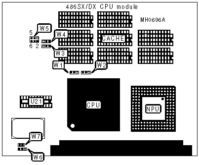
USER CONFIGURABLE SETTINGS |
|||
|
Function |
Jumper |
Position |
|
|
|
CPU type select 80486SX |
W6 |
pins 1 & 2 closed |
|
|
CPU type select 80486DX |
W6 |
pins 2 & 3 closed |
|
» |
Factory configured - do not alter |
W7 |
Closed |
|
CACHE CONFIGURATION |
||
|
Size |
Bank 0 |
U21 |
|
64KB |
(8) 16K x 4 |
(1) 16K x 4 |
|
256KB |
(8) 64K x 4 |
NONE |
|
CACHE JUMPER CONFIGURATION |
|||||
|
Size |
SW5/3 |
SW5/4 |
W1 |
W2 |
W5 |
|
64KB |
Off |
Off |
2 & 3 |
2 & 3 |
Open |
|
256KB |
On |
On |
1 & 2 |
1 & 2 |
3 & 4, 5 & 6 |
|
Note: The location of SW5 on the mainboard is unidentified. Pins designated should be in the closed position. |
|||||
|
BURST MODE CONFIGURATION |
|||
|
Setting |
W3 |
W4 |
W5 |
|
Enabled |
pins 2 & 3 closed |
pins 2 & 3 closed |
pins 1 & 2 closed |
|
Disabled |
pins 1 & 2 closed |
pins 1 & 2 closed |
Open |