EISA TECH CORPORATION
386SX
|
Processor |
80386SX |
|
Processor Speed |
16/20MHz |
|
Chip Set |
VLSI |
|
Max. Onboard DRAM |
16MB |
|
Cache |
None |
|
BIOS |
AMI |
|
Dimensions |
330mm x 218mm |
|
I/O Options |
None |
|
NPU Options |
80387SX |
|
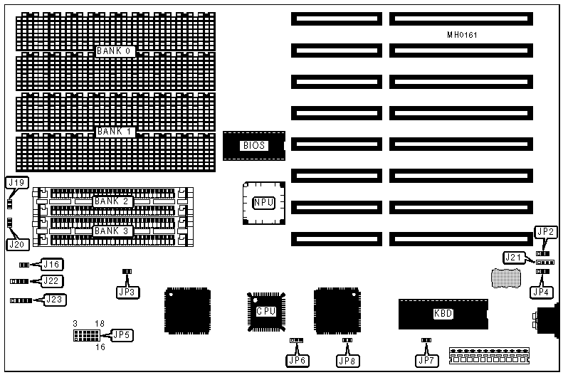
CONNECTIONS | |||
|
Purpose |
Location |
Purpose |
Location |
|
Reset switch |
J16 |
External battery |
J21 |
|
Turbo switch |
J19 |
Speaker |
J22 |
|
Turbo LED |
J20 |
Power LED & keylock |
J23 |
|
USER CONFIGURABLE SETTINGS | |||
|
Function |
Jumper |
Position | |
| » |
Battery select internal |
JP2 |
pins 1 & 2 closed |
|
Battery select external |
JP2 |
pins 2 & 3 closed | |
| » |
Pipeline mode enabled |
JP3 |
Closed |
|
Pipeline mode disabled |
JP3 |
Open | |
| » |
CMOS memory normal operation |
JP4 |
pins 1 & 2 closed |
|
CMOS memory clear |
JP4 |
pins 2 & 3 closed | |
| » |
CPU ready signal select from 82C320 |
JP6 |
pins 1 & 2 closed |
|
CPU ready signal select from NPX |
JP6 |
pins 2 & 3 closed | |
| » |
Monitor type select monochrome |
JP7 |
Open |
|
Monitor type select color |
JP7 |
Closed | |
| » |
Maximum bus amperage select 24mA |
JP8 |
Closed |
|
Maximum bus amperage select 12mA |
JP8 |
Open | |
|
DRAM CONFIGURATION | ||||
|
Size |
Bank 0 |
Bank 1 |
Bank 2 |
Bank 3 |
|
512KB |
(18) 41256 |
NONE |
NONE |
NONE |
|
512KB |
NONE |
NONE |
(2) 256K x 9 |
NONE |
|
1MB |
(18) 41256 |
(18) 41256 |
NONE |
NONE |
|
1MB |
NONE |
NONE |
(2) 256K x 9 |
(2) 256K x 9 |
|
1.5MB |
(18) 41256 |
(18) 41256 |
(2) 256K x 9 |
NONE |
|
2MB |
(18) 41256 |
(18) 41256 |
(2) 256K x 9 |
(2) 256K x 9 |
|
2MB |
(18) 411000 |
NONE |
NONE |
NONE |
|
3MB |
(18) 41256 |
(18) 41256 |
(2) 1M x 9 |
NONE |
|
4MB |
(18) 411000 |
(18) 411000 |
NONE |
NONE |
|
4.5MB |
(18) 411000 |
(18) 411000 |
(2) 256K x 9 |
NONE |
|
5MB |
(18) 411000 |
(18) 411000 |
(2) 256K x 9 |
(2) 256K x 9 |
|
5MB |
(18) 41256 |
(18) 41256 |
(2) 1M x 9 |
(2) 1M x 9 |
|
6MB |
(18) 411000 |
(18) 411000 |
(2) 1M x 9 |
NONE |
|
8MB |
(18) 411000 |
(18) 411000 |
(2) 1M x 9 |
(2) 1M x 9 |
|
8MB |
(18) 414000 |
NONE |
NONE |
NONE |
|
8MB |
NONE |
NONE |
(2) 4M x 9 |
NONE |
|
9MB |
(18) 414000 |
(18) 41256 |
(2) 4M x 9 |
NONE |
|
12MB |
(18) 411000 |
(18) 411000 |
(2) 4M x 9 |
NONE |
|
16MB |
(18) 414000 |
(18) 414000 |
NONE |
NONE |
|
16MB |
NONE |
NONE |
(2) 4M x 9 |
(2) 4M x 9 |
|
DRAM JUMPER CONFIGURATION | |
|
Size |
JP5 |
|
512KB |
pins 1 & 2, 4 & 5, 7 & 8, 10 & 11, 13 & 14, 16 & 17 closed |
|
512KB |
pins 2 & 3, 5 & 6, 8 & 9, 11 & 12, 14 & 15, 17 & 18 closed |
|
1MB |
pins 1 & 2, 4 & 5, 7 & 8, 10 & 11, 13 & 14, 16 & 17 closed |
|
1MB |
pins 2 & 3, 5 & 6, 8 & 9, 11 & 12, 14 & 15, 17 & 18 closed |
|
1.5MB |
pins 1 & 2, 4 & 5, 7 & 8, 10 & 11, 13 & 14, 16 & 17 closed |
|
2MB |
pins 1 & 2, 4 & 5, 7 & 8, 10 & 11, 13 & 14, 16 & 17 closed |
|
2MB |
pins 1 & 2, 4 & 5, 7 & 8, 10 & 11, 13 & 14, 16 & 17 closed |
|
3MB |
pins 1 & 2, 4 & 5, 7 & 8, 10 & 11, 13 & 14, 16 & 17 closed |
|
4MB |
pins 1 & 2, 4 & 5, 7 & 8, 10 & 11, 13 & 14, 16 & 17 closed |
|
4.5MB |
pins 1 & 2, 4 & 5, 7 & 8, 10 & 11, 13 & 14, 16 & 17 closed |
|
5MB |
pins 1 & 2, 4 & 5, 7 & 8, 10 & 11, 13 & 14, 16 & 17 closed |
|
5MB |
pins 1 & 2, 4 & 5, 7 & 8, 10 & 11, 13 & 14, 16 & 17 closed |
|
6MB |
pins 1 & 2, 4 & 5, 7 & 8, 10 & 11, 13 & 14, 16 & 17 closed |
|
8MB |
pins 1 & 2, 4 & 5, 7 & 8, 10 & 11, 13 & 14, 16 & 17 closed |
|
8MB |
pins 1 & 2, 4 & 5, 7 & 8, 10 & 11, 13 & 14, 16 & 17 closed |
|
8MB |
pins 2 & 3, 5 & 6, 8 & 9, 11 & 12, 14 & 15, 17 & 18 closed |
|
9MB |
pins 1 & 2, 4 & 5, 7 & 8, 10 & 11, 13 & 14, 16 & 17 closed |
|
12MB |
pins 1 & 2, 4 & 5, 7 & 8, 10 & 11, 13 & 14, 16 & 17 closed |
|
16MB |
pins 1 & 2, 4 & 5, 7 & 8, 10 & 11, 13 & 14, 16 & 17 closed |
|
16MB |
pins 2 & 3, 5 & 6, 8 & 9, 11 & 12, 14 & 15, 17 & 18 closed |
|
Note:Each line in this table corresponds to same line in the above DRAM configuration table. | |