AUVA COMPUTER, INC.
BABY 286 BAM/12-S2
|
Processor |
80286 |
|
Processor Speed |
12MHz |
|
Chip Set |
Suntac |
|
Max. Onboard DRAM |
4MB |
|
Cache |
None |
|
BIOS |
Award/Phoenix |
|
Dimensions |
330mm x 220mm |
|
I/O Options |
None |
|
NPU Options |
80287 |
|
CONNECTIONS |
|||
|
Purpose |
Location |
Purpose |
Location |
|
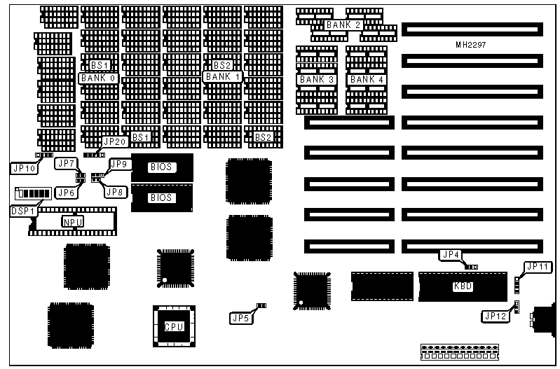
Reset switch |
JP6 |
Speaker |
JP10 |
|
Turbo switch |
JP7 |
External battery |
JP11 |
|
Turbo LED |
JP8 |
Power LED & keylock |
JP20 |
|
USER CONFIGURABLE SETTINGS |
|||
|
Function |
Jumper/Switch |
Position |
|
|
» |
Monitor type select color |
DSP1/1 |
On |
|
|
Monitor type select monochrome |
DSP1/1 |
Off |
|
» |
EMS port address 0E8H |
DSP1/2 |
On |
|
|
EMS port address 098H |
DSP1/2 |
Off |
|
» |
BIOS type select 27128 |
DSP1/3 |
On |
|
|
BIOS type select 27256 |
DSP1/3 |
Off |
|
» |
Keyboard BIOS output select pin 23 |
JP4 |
Pins 2 & 3 closed |
|
|
Keyboard BIOS output select pin 30 |
JP4 |
Pins 1 & 2 closed |
|
» |
Wait state select 0 wait state |
JP5 |
Open |
|
|
Wait state select 1-wait state |
JP5 |
Closed |
|
» |
ROM speed control disabled |
JP9 |
Pins 2 & 3 closed |
|
|
ROM speed control enabled |
JP9 |
Pins 1 & 2 closed |
|
» |
Battery type select internal |
JP12 |
Pins 1 & 2 closed |
|
|
Battery type select external |
JP12 |
Pins 2 & 3 closed |
|
DRAM MODE CONFIGURATION |
||||
|
Mode |
Total |
Base |
Extended |
Expanded |
|
0 |
512KB |
512KB |
0KB |
0KB |
|
1 |
640KB |
640KB |
0KB |
0KB |
|
2 |
1MB |
640KB |
384KB |
0KB |
|
3 |
1MB |
640KB |
0KB |
384KB |
|
4 |
2MB |
640KB |
1408KB |
0KB |
|
5 |
2MB |
640KB |
0KB |
1408KB |
|
6 |
4MB |
640KB |
3456KB |
0KB |
|
7 |
4MB |
640KB |
0KB |
3456KB |
|
DRAM CONFIGURATION |
|||||
|
Mode |
Bank 0 |
Bank 1 |
Bank 2 |
Bank 3 |
Bank 4 |
|
0 |
(18) 41256 |
NONE |
NONE |
NONE |
NONE |
|
0 |
(2) 41256 |
NONE |
NONE |
(4) 44256 |
NONE |
|
1 |
(18) 41256 |
(18) 4164 |
NONE |
NONE |
NONE |
|
1 |
(2) 41256 |
(2) 4164 |
(4) 4464 |
(4) 44256 |
NONE |
|
2 |
(18) 41256 |
(18) 41256 |
NONE |
NONE |
NONE |
|
2 |
(2) 41256 |
(2) 41256 |
NONE |
(4) 44256 |
(4) 44256 |
|
3 |
(18) 41256 |
(18) 41256 |
NONE |
NONE |
NONE |
|
3 |
(2) 41256 |
(2) 41256 |
NONE |
(4) 44256 |
(4) 44256 |
|
4 |
(18) 411000 |
NONE |
NONE |
NONE |
NONE |
|
5 |
(18) 411000 |
NONE |
NONE |
NONE |
NONE |
|
6 |
(18) 411000 |
(18) 411000 |
NONE |
NONE |
NONE |
|
7 |
(18) 411000 |
(18) 411000 |
NONE |
NONE |
NONE |
|
Note: When there are 2 chips in Bank 0 or Bank 1, they are placed in BS1 and BS2 respectively. |
|||||
|
DRAM SWITCH CONFIGURATION |
|||
|
Mode |
DSP1/4 |
DSP1/5 |
DSP1/6 |
|
0 |
On |
On |
On |
|
1 |
On |
On |
Off |
|
2 |
On |
Off |
On |
|
3 |
On |
Off |
Off |
|
4 |
Off |
On |
On |
|
5 |
Off |
On |
Off |
|
6 |
Off |
Off |
On |
|
7 |
Off |
Off |
Off |