QUATECH, INC.
DSDP-402
|
Card Type |
Multi I/O |
|
Chipset Controller |
Unidentified |
|
I/O Options |
Serial ports (2), parallel ports (2) |
|
Maximum Dram |
N/A |
|
CONNECTIONS | |
|
Purpose |
Location |
|
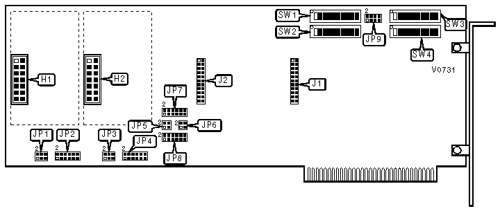
Serial controller daughtercard 1 header |
H1 |
|
Serial controller daughtercard 2 header |
H2 |
|
Parallel port 1 |
J1 |
|
Parallel port 2 |
J2 |
|
SERIAL PORT CONFIGURATION | |||
|
Port 1 |
Port 2 |
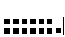
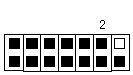
JP9 pins 1 & 2 |
JP9 pins 3 & 4 |
|
Enabled |
Enabled |
Closed |
Closed |
|
Enabled |
Disabled |
Closed |
Open |
|
Disabled |
Enabled |
Open |
Closed |
|
Disabled |
Disabled |
Open |
Open |
|
SERIAL INTERRUPT SHARING | |||
|
Port 1 IRQ |
Port 2 IRQ |
JP1 |
JP3 |
|
Non-sharable |
Non-sharable |
Pins 1 & 2 closed |
Pins 1 & 2 closed |
|
Non-sharable |
Sharable |
Pins 1 & 2 closed |
Pins 3 & 4, 5 & 6 closed |
|
Sharable |
Non-sharable |
Pins 3 & 4, 5 & 6 closed |
Pins 1 & 2 closed |
|
Sharable |
Sharable |
Pins 3 & 4, 5 & 6 closed |
Pins 3 & 4, 5 & 6 closed |
|
SERIAL PORT 1 ADDRESS SELECTION | ||||||||||
|
Address |
SW1/10 |
SW1/9 |
SW1/8 |
SW1/7 |
SW1/6 |
SW1/5 |
SW1/4 |
SW1/3 |
SW1/2 |
SW1/1 |
|
000h |
On |
On |
On |
On |
On |
On |
On |
On |
On |
On |
|
001h |
On |
On |
On |
On |
On |
On |
On |
On |
On |
Off |
|
002h |
On |
On |
On |
On |
On |
On |
On |
On |
Off |
On |
|
003h |
On |
On |
On |
On |
On |
On |
On |
On |
Off |
Off |
|
004h |
On |
On |
On |
On |
On |
On |
On |
Off |
On |
On |
|
2E8h (COM4) |
Off |
On |
Off |
Off |
Off |
On |
Off |
On |
On |
On |
|
2F8h (COM2) |
Off |
On |
Off |
Off |
Off |
Off |
Off |
On |
On |
On |
|
3E8h (COM3) |
Off |
Off |
Off |
Off |
Off |
On |
Off |
On |
On |
On |
|
3F4h |
Off |
Off |
Off |
Off |
Off |
Off |
On |
Off |
On |
On |
|
3F5h |
Off |
Off |
Off |
Off |
Off |
Off |
On |
Off |
On |
Off |
|
3F6h |
Off |
Off |
Off |
Off |
Off |
Off |
On |
Off |
Off |
On |
|
3F7h |
Off |
Off |
Off |
Off |
Off |
Off |
On |
Off |
Off |
Off |
|
3F8h (COM1) |
Off |
Off |
Off |
Off |
Off |
Off |
Off |
On |
On |
On |
|
Note: A total of 1023 memory base address settings are available. The switches are a binary representation of the decimal addresses. Switch 1 is the Least Significant Bit and switch 10 is the Most Significant Bit. The switches have the following decimal values: switch 1=1, 2=2, 3=4, 4=8, 5=16, 6=32, 7=64, 8=128, 9=256, 10=512. Add the values of the off switches to obtain the correct memory address. (On=0, Off=1) | ||||||||||
|
SERIAL PORT 1 ADDRESS SELECTION | ||||||||||
|
Address |
SW2/10 |
SW2/9 |
SW2/8 |
SW2/7 |
SW2/6 |
SW2/5 |
SW2/4 |
SW2/3 |
SW2/2 |
SW2/1 |
|
000h |
On |
On |
On |
On |
On |
On |
On |
On |
On |
On |
|
001h |
On |
On |
On |
On |
On |
On |
On |
On |
On |
Off |
|
002h |
On |
On |
On |
On |
On |
On |
On |
On |
Off |
On |
|
003h |
On |
On |
On |
On |
On |
On |
On |
On |
Off |
Off |
|
004h |
On |
On |
On |
On |
On |
On |
On |
Off |
On |
On |
|
2E8h (COM4) |
Off |
On |
Off |
Off |
Off |
On |
Off |
On |
On |
On |
|
2F8h (COM2) |
Off |
On |
Off |
Off |
Off |
Off |
Off |
On |
On |
On |
|
3E8h (COM3) |
Off |
Off |
Off |
Off |
Off |
On |
Off |
On |
On |
On |
|
3F4h |
Off |
Off |
Off |
Off |
Off |
Off |
On |
Off |
On |
On |
|
3F5h |
Off |
Off |
Off |
Off |
Off |
Off |
On |
Off |
On |
Off |
|
3F6h |
Off |
Off |
Off |
Off |
Off |
Off |
On |
Off |
Off |
On |
|
3F7h |
Off |
Off |
Off |
Off |
Off |
Off |
On |
Off |
Off |
Off |
|
3F8h (COM1) |
Off |
Off |
Off |
Off |
Off |
Off |
Off |
On |
On |
On |
|
Note: A total of 1023 memory base address settings are available. The switches are a binary representation of the decimal addresses. Switch 1 is the Least Significant Bit and switch 10 is the Most Significant Bit. The switches have the following decimal values: switch 1=1, 2=2, 3=4, 4=8, 5=16, 6=32, 7=64, 8=128, 9=256, 10=512. Add the values of the off switches to obtain the correct memory address. (On=0, Off=1) | ||||||||||
|
SERIAL PORT 1 IRQ SELECTION | |
|
IRQ |
JP2 |
|
2 |
Pins 1 & 2 closed |
|
3 |
Pins 3 & 4 closed |
|
4 |
Pins 5 & 6 closed |
|
5 |
Pins 7 & 8 closed |
|
6 |
Pins 9 & 10 closed |
|
7 |
Pins 11 & 12 closed |
|
SERIAL PORT 2 IRQ SELECTION | |
|
IRQ |
JP4 |
|
2 |
Pins 1 & 2 closed |
|
3 |
Pins 3 & 4 closed |
|
4 |
Pins 5 & 6 closed |
|
5 |
Pins 7 & 8 closed |
|
6 |
Pins 9 & 10 closed |
|
7 |
Pins 11 & 12 closed |
|
PARALLEL PORT CONFIGURATION | |||
|
Port 1 |
Port 2 |
JP9 pins 5 & 6 |
JP9 pins 7 & 8 |
|
Enabled |
Enabled |
Closed |
Closed |
|
Enabled |
Disabled |
Closed |
Open |
|
Disabled |
Enabled |
Open |
Closed |
|
Disabled |
Disabled |
Open |
Open |
|
PARALLEL PORT INTERRUPT LEVEL SELECTION | |||
|
Port 1 mode |
Port 2 mode |
JP5 |
JP6 |
|
High-Low-High |
High-Low-High |
Pins 1 & 2 closed |
Pins 1 & 2 closed |
|
High-Low-High |
Low-High-Low |
Pins 1 & 2 closed |
Pins 3 & 4 closed |
|
Low-High-Low |
High-Low-High |
Pins 3 & 4 closed |
Pins 1 & 2 closed |
|
Low-High-Low |
Low-High-Low |
Pins 3 & 4 closed |
Pins 3 & 4 closed |
|
PARALLEL PORT DIRECTION SELECTION | |||
|
Port 1 mode |
Port 2 mode |
JP10 |
jP11 |
|
Bidirectional |
Bidirectional |
Pins 3 & 4 closed |
Pins 3 & 4 closed |
|
Bidirectional |
Unidirectional |
Pins 3 & 4 closed |
Pins 1 & 2 closed |
|
Unidirectional |
Bidirectional |
Pins 1 & 2 closed |
Pins 3 & 4 closed |
|
Unidirectional |
Unidirectional |
Pins 1 & 2 closed |
Pins 1 & 2 closed |
|
PARALLEL PORT 1 ADDRESS SELECTION | ||||||||||
|
Address |
SW3/9 |
SW3/8 |
SW3/7 |
SW3/6 |
SW3/5 |
SW3/4 |
SW3/3 |
SW3/2 |
SW3/1 |
SW3/0 |
|
000h |
On |
On |
On |
On |
On |
On |
On |
On |
On |
On |
|
001h |
On |
On |
On |
On |
On |
On |
On |
On |
On |
Off |
|
002h |
On |
On |
On |
On |
On |
On |
On |
On |
Off |
On |
|
003h |
On |
On |
On |
On |
On |
On |
On |
On |
Off |
Off |
|
004h |
On |
On |
On |
On |
On |
On |
On |
Off |
On |
On |
|
278h (LPT2) |
Off |
On |
On |
Off |
Off |
Off |
Off |
On |
On |
On |
|
378h (LPT1) |
Off |
Off |
On |
Off |
Off |
Off |
Off |
On |
On |
On |
|
3BCh (LPT3) |
Off |
Off |
Off |
On |
Off |
Off |
Off |
Off |
On |
On |
|
3F4h |
Off |
Off |
Off |
Off |
Off |
Off |
On |
Off |
On |
On |
|
3F5h |
Off |
Off |
Off |
Off |
Off |
Off |
On |
Off |
On |
Off |
|
3F6h |
Off |
Off |
Off |
Off |
Off |
Off |
On |
Off |
Off |
On |
|
3F7h |
Off |
Off |
Off |
Off |
Off |
Off |
On |
Off |
Off |
Off |
|
3F8h |
Off |
Off |
Off |
Off |
Off |
Off |
Off |
On |
On |
On |
|
Note: A total of 1023 memory base address settings are available. The switches are a binary representation of the decimal addresses. Switch 1 is the Least Significant Bit and switch 10 is the Most Significant Bit. The switches have the following decimal values: switch 1=1, 2=2, 3=4, 4=8, 5=16, 6=32, 7=64, 8=128, 9=256, 10=512. Add the values of the off switches to obtain the correct memory address. (On=0, Off=1) | ||||||||||
|
PARALLEL PORT 2 ADDRESS SELECTION | ||||||||||
|
Address |
SW4/9 |
SW4/8 |
SW4/7 |
SW4/6 |
SW4/5 |
SW4/4 |
SW4/3 |
SW4/2 |
SW4/1 |
SW4/0 |
|
000h |
On |
On |
On |
On |
On |
On |
On |
On |
On |
On |
|
001h |
On |
On |
On |
On |
On |
On |
On |
On |
On |
Off |
|
002h |
On |
On |
On |
On |
On |
On |
On |
On |
Off |
On |
|
003h |
On |
On |
On |
On |
On |
On |
On |
On |
Off |
Off |
|
004h |
On |
On |
On |
On |
On |
On |
On |
Off |
On |
On |
|
278h (LPT2) |
Off |
On |
On |
Off |
Off |
Off |
Off |
On |
On |
On |
|
378h (LPT1) |
Off |
Off |
On |
Off |
Off |
Off |
Off |
On |
On |
On |
|
3BCh (LPT3) |
Off |
Off |
Off |
On |
Off |
Off |
Off |
Off |
On |
On |
|
3F4h |
Off |
Off |
Off |
Off |
Off |
Off |
On |
Off |
On |
On |
|
3F5h |
Off |
Off |
Off |
Off |
Off |
Off |
On |
Off |
On |
Off |
|
3F6h |
Off |
Off |
Off |
Off |
Off |
Off |
On |
Off |
Off |
On |
|
3F7h |
Off |
Off |
Off |
Off |
Off |
Off |
On |
Off |
Off |
Off |
|
3F8h |
Off |
Off |
Off |
Off |
Off |
Off |
Off |
On |
On |
On |
|
Note: A total of 1023 memory base address settings are available. The switches are a binary representation of the decimal addresses. Switch 1 is the Least Significant Bit and switch 10 is the Most Significant Bit. The switches have the following decimal values: switch 1=1, 2=2, 3=4, 4=8, 5=16, 6=32, 7=64, 8=128, 9=256, 10=512. Add the values of the off switches to obtain the correct memory address. (On=0, Off=1) | ||||||||||
|
PARALLEL PORT 1 IRQ SELECTION | |
|
IRQ |
JP7 |
|
2 |
Pins 1 & 2 closed |
|
3 |
Pins 3 & 4 closed |
|
4 |
Pins 5 & 6 closed |
|
5 |
Pins 7 & 8 closed |
|
6 |
Pins 9 & 10 closed |
|
7 |
Pins 11 & 12 closed |
|
PARALLEL PORT 2 IRQ SELECTION | |
|
IRQ |
JP8 |
|
2 |
Pins 1 & 2 closed |
|
3 |
Pins 3 & 4 closed |
|
4 |
Pins 5 & 6 closed |
|
5 |
Pins 7 & 8 closed |
|
6 |
Pins 9 & 10 closed |
|
7 |
Pins 11 & 12 closed |
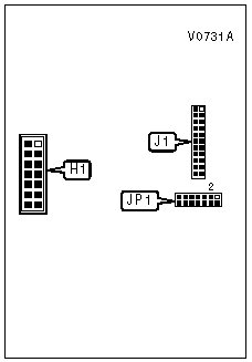
DRV-232 DAUGHTERBOARD
|
CONNECTIONS | |
|
Purpose |
Location |
|
Header to mainboard |
H1 |
|
Serial port |
J1 |
|
DTE/DCE CONFIGURATION | |
|
DTE |
DCE |
|
JP1
|
JP1
|
DRV-422/DRV-485 DAUGHTERBOARD
|
CONNECTIONS | |
|
Purpose |
Location |
|
Header to mainboard |
H1 |
|
Serial port |
J1 |
|
DUPLEX CONFIGURATION | |
|
Setting |
JP1, pins 3 & 6 |
|
Half |
Closed |
|
Full |
Open |
|
RTS/CTS CONFIGURATION | |
|
Pass-thorugh |
Loopback |
|
JP1
|
JP1
|