INNOVATIVE INTEGRATION
PC44
|
Card Type |
Digital I/O card, DSP processor card |
|
Chip Set |
TI |
|
Maximum Onboard Memory |
8MB SRAM |
|
I/O Options |
Com ports (6), Analog I/O, Digital I/O, Factory test port |
|
Data Bus |
16-bit ISA |
|
Card Size |
Full-length, full-height card |
|
CONNECTIONS |
|||
|
Function |
Label |
Function |
Label |
|
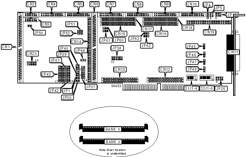
Unidentified |
CN1 |
Analog I/O |
CN11 |
|
Unidentified |
CN2 |
Unidentified |
CN12 |
|
Unidentified |
CN3 |
Unidentified |
CN13 |
|
Processor A com 1 |
CN4 |
Unidentified |
CN14 |
|
Processor A com 2 |
CN5 |
Unidentified |
CN15 |
|
Unidentified |
CN6 |
Unidentified |
CN16 |
|
Processor B com 1 |
CN7 |
Unidentified |
CN17 |
|
Processor B com 2 |
CN8 |
Unidentified |
CN18 |
|
Processor C com 1 |
CN9 |
Digital I/O |
CN19 |
|
Processor C com 2 |
CN10 |
Factory test port - do not use |
CN20 |
|
USER CONFIGURABLE SETTINGS |
|||
|
Function |
Label |
Position |
|
|
» |
JTAG IN/OUT to TIM site A |
JP1 |
Closed |
|
|
JTAG IN/OUT not TIM site A |
JP1 |
Open |
|
» |
Digital I/O latch clock internal |
JP4 |
Pins 2 & 3 closed |
|
|
Digital I/O latch clock external |
JP4 |
Pins 1 & 2 closed |
|
» |
Digital I/O direction 0-15=output |
JP5 |
Pins 1 & 3 closed |
|
» |
Digital I/O direction 16-31=output |
JP5 |
Pins 2 & 4 closed |
|
» |
JTAG IN/OUT to TIM site B |
JP30 |
Closed |
|
|
JTAG IN/OUT not TIM site B |
JP30 |
Open |
|
» |
JTAG passthru disabled |
JP50 |
Closed |
|
|
JTAG passthru enabled |
JP50 |
Open |
|
» |
4Xbus strobe A_STRB0 |
JP64 |
Pins 2 & 3 closed |
|
|
4Xbus strobe GYBANK1 |
JP64 |
Pins 1 & 2 closed |
|
DRAM CONFIGURATION |
|
|
Size |
Bank 0 |
|
128KB |
(2) 32KB x 32 |
|
256KB |
(2) 64KB x 32 |
|
512KB |
(2) 128KB x 32 |
|
1MB |
(2) 256KB x 32 |
|
2MB |
(2) 512KB x 32 |
|
4MB |
(2) 1MB x 32 |
|
8MB |
(2) 2MB x 32 |
|
TIMER SOURCE 0 SELECTION |
||
|
Setting |
JP39 |
|
|
|
Processor A TCLK0 |
Pins 1 & 3 closed |
|
» |
82C54 channel 0 |
Pins 3 & 5 closed |
|
|
82C54 channel 1 |
Pins 2 & 4 closed |
|
|
82C54 channel 2 |
Pins 4 & 6 closed |
|
TIMER SOURCE 1 SELECTION |
||
|
Setting |
JP40 |
|
|
|
Processor A TCLK0 |
Pins 1 & 3 closed |
|
|
82C54 channel 0 |
Pins 3 & 5 closed |
|
» |
82C54 channel 1 |
Pins 2 & 4 closed |
|
|
82C54 channel 2 |
Pins 4 & 6 closed |
|
D/A TRIGGER SELECTION |
||
|
Setting |
JP37 |
|
|
|
D/A1=EXT TM SRC0 |
Pins 1 & 2 closed |
|
» |
D/A0 & DAC1 driven as pair |
Pins 3 & 4 closed |
|
|
D/A0= TM SRC 0 |
Pins 5 & 6 closed |
|
» |
All D/A channels driven as a quad |
Pins 7 & 8, 3 & 4, 11 & 12 closed |
|
|
D/A2 = TM SRC1 |
Pins 9 & 10 closed |
|
|
D/A2 & DAC3 driven as pair |
Pins 11 & 12 closed |
|
|
D/A3 = EXT TM SCR1 |
Pins 13 & 14 closed |
|
DAC 0 OUTPUT RANGE SELECTION |
|
|
Range |
JP46 |
|
0-10V |
Pins 1 & 2 closed |
|
+-10V |
Pins 2 & 3 closed |
|
DAC 1 OUTPUT RANGE SELECTION |
|
|
Range |
JP45 |
|
0-10V |
Pins 1 & 2 closed |
|
+-10V |
Pins 2 & 3 closed |
|
DAC 2 OUTPUT RANGE SELECTION |
|
|
Range |
JP48 |
|
0-10V |
Pins 1 & 2 closed |
|
+-10V |
Pins 2 & 3 closed |
|
DAC 3 OUTPUT RANGE SELECTION |
|
|
Range |
JP47 |
|
0-10V |
Pins 1 & 2 closed |
|
+-10V |
Pins 2 & 3 closed |
|
82C54 CLOCK SOURCE SELECTION |
|
|
Setting |
JP15 |
|
CLK0 = H1/4 |
Pins 1 & 2 closed |
|
CLK1 = H1/4 |
Pins 3 & 4 closed |
|
CLK2 = H1/4 |
Pins 5 & 6 closed |
|
PROCESSOR A INTERRUPTS EINT0 |
|
|
Setting |
JP43 |
|
Ext Int 0 |
Pins 1 & 3 closed |
|
Dport Int |
Pins 3 & 5 closed |
|
TM_SRC0 |
Pins 2 & 4 closed |
|
EXT_TM_SRC0 |
Pins 4 & 6 closed |
|
PROCESSOR A INTERRUPTS EINT1 |
|
|
Setting |
JP43 |
|
Ext Int 1 |
Pins 7 & 9 closed |
|
ADC_A_NOT_BUSY |
Pins 9 & 11 closed |
|
TM_SRC1 |
Pins 8 & 10 closed |
|
ADC_B_NOT_BUSY |
Pins 10 & 12 closed |
|
PROCESSOR A INTERRUPTS EINT2 |
|
|
Setting |
JP43 |
|
Ext Int 2 |
Pins 13 & 15 closed |
|
Int B to A |
Pins 15 & 17 closed |
|
PC_INT0 |
Pins 14 & 16 closed |
|
EXT_TM_SRC1 |
Pins 16 & 18 closed |
|
PROCESSOR B INTERRUPTS EINT0 |
|
|
Setting |
JP41 |
|
Ext Int 0 |
Pins 1 & 3 closed |
|
Dport Int |
Pins 3 & 5 closed |
|
TM_SRC0 |
Pins 2 & 4 closed |
|
EXT_TM_SRC0 |
Pins 4 & 6 closed |
|
PROCESSOR B INTERRUPTS EINT1 |
|
|
Setting |
JP41 |
|
Ext Int 1 |
Pins 7 & 9 closed |
|
ADC_A_NOT_BUSY |
Pins 9 & 11 closed |
|
TM_SRC1 |
Pins 8 & 10 closed |
|
ADC_B_NOT_BUSY |
Pins 10 & 12 closed |
|
PROCESSOR B INTERRUPTS EINT2 |
|
|
Setting |
JP41 |
|
Ext Int 2 |
Pins 13 & 15 closed |
|
Int A to B |
Pins 15 & 17 closed |
|
PC_INT1 |
Pins 14 & 16 closed |
|
EXT_TM_SRC1 |
Pins 16 & 18 closed |
|
PROCESSOR C INTERRUPTS EINT0 |
|
|
Setting |
JP42 |
|
Ext Int 0 |
Pins 1 & 3 closed |
|
Dport Int |
Pins 3 & 5 closed |
|
TM_SRC0 |
Pins 2 & 4 closed |
|
EXT_TM_SRC0 |
Pins 4 & 6 closed |
|
PROCESSOR C INTERRUPTS EINT1 |
|
|
Setting |
JP42 |
|
Ext Int 1 |
Pins 7 & 9 closed |
|
ADC_A_NOT_BUSY |
Pins 9 & 11 closed |
|
TM_SRC1 |
Pins 8 & 10 closed |
|
ADC_B_NOT_BUSY |
Pins 10 & 12 closed |
|
PROCESSOR C INTERRUPTS EINT2 |
|
|
Setting |
JP42 |
|
Ext Int 2 |
Pins 13 & 15 closed |
|
Ext Int 3 |
Pins 15 & 17 closed |
|
PC_INT2 |
Pins 14 & 16 closed |
|
EXT_TM_SRC1 |
Pins 16 & 18 closed |
|
A/D TRIGGER SELECTION |
||
|
Setting |
JP38 |
|
|
|
A/D A = EXT TM_SRC0 |
Pins 1 & 3 closed |
|
|
A/D A = software |
Pins 2 & 4 closed |
|
» |
A/D A = TM SCR 0 |
Pins 3 & 5 closed |
|
» |
Channels A & B |
Pins 6 & 8 closed |
|
|
A/D B = TM SRC 1 |
Pins 7 & 9 closed |
|
|
A/C B = EXT TM SRC 1 |
Pins 9 & 11 closed |
|
|
A/D B = software |
Pins 10 & 12 closed |
|
PC INTERRUPT SELECTION |
|
|
IRQ |
JP25 |
|
5 |
Pins 1 & 2 closed |
|
7 |
Pins 3 & 4 closed |
|
11 |
Pins 5 & 6 closed |
|
15 |
Pins 7 & 8 closed |
|
I/O ADDRESS |
||||
|
Address |
S1/1 |
S1/2 |
S1/3 |
S1/4 |
|
0x280h |
On |
Off |
On |
On |
|
DPORT ADDRESS |
||||||
|
Address |
S2/1 |
S2/2 |
S2/3 |
S2/4 |
S2/5 |
S2/6 |
|
0xD0000h |
Off |
Off |
On |
Off |
On |
On |
|
PROCESSOR A PORT 5 SETTING |
|||
|
Setting |
Label |
Position |
|
|
» |
Processor A com port 5 bi-directional |
JP51 |
Pins 1 & 2 closed |
|
|
Processor A com port 5 uni-directional |
JP51 |
Open |
|
|
Reserved |
JP51 |
Pins 2 & 3 closed |
|
PROCESSOR A PORT 2 SETTING |
|||
|
Setting |
Label |
Position |
|
|
» |
Processor A com port 2 bi-directional |
JP52 |
Pins 1 & 2 closed |
|
|
Processor A com port 2 uni-directional |
JP52 |
Open |
|
|
Reserved |
JP52 |
Pins 2 & 3 closed |
|
PROCESSOR B PORT 5 SETTING |
|||
|
Setting |
Label |
Position |
|
|
» |
Processor B com port 5 bi-directional |
JP60 |
Pins 1 & 2 closed |
|
|
Processor B com port 5 uni-directional |
JP60 |
Open |
|
|
Reserved |
JP60 |
Pins 2 & 3 closed |
|
PROCESSOR B PORT 2 SETTING |
|||
|
Setting |
Label |
Position |
|
|
» |
Processor B com port 2 bi-directional |
JP61 |
Pins 1 & 2 closed |
|
|
Processor B com port 2 uni-directional |
JP61 |
Open |
|
|
Reserved |
JP61 |
Pins 2 & 3 closed |
|
PROCESSOR C PORT 5 SETTING |
|||
|
Setting |
Label |
Position |
|
|
» |
Processor C com port 5 bi-directional |
JP62 |
Pins 1 & 2 closed |
|
|
Processor C com port 5 uni-directional |
JP62 |
Open |
|
|
Reserved |
JP62 |
Pins 2 & 3 closed |
|
PROCESSOR C PORT 2 SETTING |
|||
|
Setting |
Label |
Position |
|
|
» |
Processor C com port 2 bi-directional |
JP63 |
Pins 1 & 2 closed |
|
|
Processor C com port 2 uni-directional |
JP63 |
Open |
|
|
Reserved |
JP63 |
Pins 2 & 3 closed |